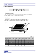
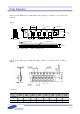
Chip Resistor ■ PACKAGING ● PACKAGING METHOD Packaging protects the resistor from damage during the shipping or storage. There are two types of packaging method ; one is "Reel" type, and the other is "Bulk" type. ● REEL TYPE PACKAGING SPECIFICATION The packaging specification is based on the EIAJ RC-1009. is tape dimension For 0603, 1005 type. is for pocket sizes, A and B. 4.0±0.1 0.1 1.5±0 1.75±0.1 1.0 3.5±0.05 B 2.0±0.05 0.5 Max Top Tape 8.0±0.1 A Chip Resistor 0.Chip Resistor is tape dimension For 1608, 2012, 3216, 3225 type. is for pocket sizes, A and B. 4.0±0.1 0.1 1.5±0 1.75±0.1 1.0 3.5±0.05 8.0±0.1 B 2.0±0.05 1.0 Max 4.0±0.1 Top Tape A Chip Resistor 1.0 Max Carrier Tape Bottom Tape is tape dimension For 5025, 6432 type. is for pocket sizes, A and B. t MAX = 1.Chip Resistor ● TAPING METHOD There are empty holes at both start part and end part of carrier tape. Reel Packed Part Empty Part Lead Part Adhesion Tape Empty Portion 10 Pitches or more ** 5,000 Pitches or 20,000 Pitches Empty Portion Lead Part Start End **** Chips *** 10 Pitches or more 200~250 mm Note ① The resistor should move in the pocket freely. ② The resistor should not adhere to the top or bottom tape. ③ There should be no vacant pocket.
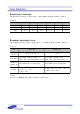
Chip Resistor ● REEL DIMENSION The Reel dimension is classified by the diameter of Reel. [ Unit : mm ] < Table 6 > Packaging Code Diameter A B C D C S 7" 178 Φ 70 9.5(13.0) ± 0.1 1.2 ± 0.1 E S 10" 258 Φ 80 9.5 ± 0.1 2.0 ± 0.1 F S, A S 13" 330 Φ 80 9.5 ± 0.1 2.0 ± 0.1 ● BULK TYPE PACKAGING Bulk cassette specification is based on the EIAJ ET-7201. The standard packaging quantity depends on the dimension. 6.0 ± 0.05 4.4 ± 0.05 3.Chip Resistor ● LABELING ▶ Reel type Label The reel type label includes following contents as . ① ② 100 - Following ① Resistance Value ② Tolerance, Marking ③ Part Number ④ Quantity ⑤ LOT Number ⑥ Bar - Code ⑦ Serial Number ③ ④ ⑤ Ohm J101 P/N : RC1608J101CS QTY : 5000PCS L/N : RMBA20630 ⑦ 007 V-2 ⑥ SAMSUNG ELECTRO-MECHANICS CO.,LTD. ▶ Bulk type Label The bulk type label includes following contents as .
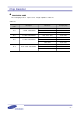
Chip Resistor ● BOX DIMENSION FOR REEL TYPE ① Max 25,000 pcs ( 5 EA × 7" ) ② Max 100,000 pcs ( 20 EA × 7" ) 30±1.0 185±1.0 195±5.0 187±5.0 66±1.0 285±5.0 185±1.0 ( Unit : mm ) ③ Max 300,000 pcs ( 60 EA ×7" ) ( Unit : mm ) ④ Max 400,000 pcs ( 20 EA ×13" ) 215±5.0 348±5.0 370±5.0 336±5.0 410±5.0 339±5.
Chip Resistor ■ RELIABILITY TEST DATA Jumper's reliability test data are only applied to General type resistor. ● ELECTRICAL CHARACTERISTIC The electrical characteristic test should satisfy the test method, procedure, and standard. If there is no special comment, Each test performs in standard state. (temperature 20℃, humidity 65%RH, pressure 1023mbar) Permissible deviation item Test method Resistor Jumper 묤 Standard : JIS C 5202 (5.1) 묤 Test voltage :
묤 Applying time : within 5 seconds.Chip Resistor Permissible deviation item Test method Resistor Withstanding voltage Insulation resistance 묤 No mechanical damage, short circuit, Jumper Same as left or disconnection. 묤 Should have more Same as than 1,000MΩ left 묤 Noise standard Noise 묤 Standard : JIS C 5202. (5.6) 묤 Test voltage : 1005 1608 DC 100V, others DC 500V 묤 Applying time : 60 seconds 묤 Test pressure : 1.0±0.2 N 묤 Test board : 묤 Standard : JIS C 5202. (5.9) Range (Ω) 묤 Standard : JIS C 5202. (5.Chip Resistor Permissible deviation item Test method Resistor Termination strength Jumper 묤 No mechanical damage, or sign of 묤 Standard : JIS C 5202 (6.1) Same as left disconnection soldering heat 묤 Standard : JIS C 5202 (6.4) 50mΩ damage 2. ΔR should be Maximum within ±(1%+0.05Ω) 2. ΔR should be 묤 Test time : 10 ± 1second (both side dipping) 묤 Standard : JIS C 5202 (6.3) 50mΩ damage 묤 Temperature : 260 ± 5℃ 묤 Test procedure : measures after 24 hours 1.
Chip Resistor Permissible deviation item Test method Resistor Low temperature exposure High temperatur exposure Jumper 1. No mechanical 50mΩ damage 2. ΔR should be Maximum within ±(3%+0.1Ω) 1. No mechanical 50mΩ damage 2. ΔR should be Maximum within ±(3%+0.1Ω) 1. No mechanical damage 2. ΔR should be within
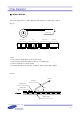
Load life Range(Ω) Standard : JIS C 5202 (7.Chip Resistor ▶ Test board ▷ Test board
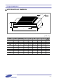
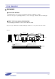
item c Dimension (mm) Dimension Power 0603 1005 1608 2012 3216 3225 5025 6432 1/20W 1/16W 1/10W 1/8W 1/4W 1/4W 1/2W 1W a 0.3 0.6 1.0 1.2 2.2 2.2 3.6 5.2 b 1.4 1.9 3.0 4.0 5.0 5.0 7.0 8.0 c 0.3 0.7 1.2 1.65 2.0 2.9 3.0 3.5 10 - φ1.0 3 3.5 f 5.2 4.9 4.5 4.3 3.3 3.3 3.0 2.5 f a b 25 5.5 7.5 5.08 3 Connector 58.5 : COPPER PATTERN : SOLDER - RESISTOR , are dimensions of test board.Chip Resistor ■ CHARACTERISTIC GRAPH ● RESISTANCE RANGE The Resistance Range that we produce depends on the Dimension and the Resistance Tolerance of the resistor.
Dimension Tolerance 0603 1005 1608 2012 3216 3225 5025 6432 (0201) (0402) (0603) (0805) (1206) (1210) (2010) (2512) Type 10Ω∼1MΩ 10Ω∼1MΩ 10Ω∼1MΩ 10Ω∼1MΩ 10Ω∼1MΩ 10Ω∼1MΩ 10Ω∼1MΩ P 0.1Ω∼1MΩ 0.1Ω∼1MΩ 0.1Ω∼1MΩ 0.1Ω∼1MΩ 0.Chip Resistor ● RATED POWER The Rated Power is classified by the dimension of the resistor.
Dimension item 0603 1005 1608 2012 3216 3225 5025 6432 (0201) (0402) (0603) (0805) (1206) (1210) (2010) (2512) 1/4 W (0.25 W) 1/2 W (0.5W) 1.0 W 1/20 W 1/16 W 1/10 W 1/8 W 1/4 W (0.05 W) (0.063 W) (0.100 W) (0.125 W) (0.25 W) Rated Power Working Volt.(Max.) 25 V 50 V 50 V 150 V 200 V 200 V 200 V 200 V STOL, IOL Volt.(Max.Chip Resistor ■ APPLICATION MANUAL ● Applications Chip resistors are designed for general electronic devices such as home appliances, computer, mobile communications, digital circuit, etc. If you require our products with high reliability-performing at more than 125C or below -55C- for medical equipments, aircraft, high speed machines, military usage, and items that can affect human life or if you need to use in specific conditions (corrosive gas atmosphere), please contact us beforehand.
Chip Resistor ● Soldering Our products have Ag electrodes protected by double layer. ▶ 1st Ni Coating - This prevents Ag electrode from leaching and enhance the bonding with Sn-Pb. ▶ 2nd Sn-Pb Coating - This is made of Sn 90% and Pb 10% with melting point 213℃ to prevent it from melting when solder cream melts, and to enhance the bonding. - Commercial solder creams are made of Sn 63% and Pb 37% with melting point 183℃.
Chip Resistor ■ NOTICE ● Usage of the resistor ▶ Flow Soldering After sticking the resistor to PCB with paste, dip the PCB into solder bath. Temp. 235±5℃ ΔT≤150℃ Pre-heating Soldering Cooling within 5 sec Time ▶ Reflow Soldering After printing solder creams on PCB, place the resistor on the solder cream. Then heat the PCB. Temp. Peak temp.