
Datasheet
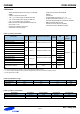
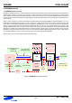
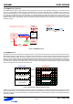
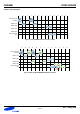
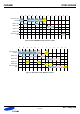
Table Of Contents

Rev. 1.4 May 2009
FBDIMM
DDR2 SDRAM
7 of 42
2.3 FBDIMM Clocking Scheme
In FB-DIMM platform design, phase adjustment among reference clock inputs to each individual AMB and host is not taken account.
Thus, clock synchronization is made by using both external reference clock and channel data stream in FB-DIMM memory system. Host
and each individual AMB has a each individual IO basis clock recovery circuitry for channel data communication. It runs with inputs from
PLL inside chip and data stream from the other AMB or Host. Because data stream itself involves data communication process, no sig-
naling switching or data communication may loss clock synchronization between transmitter and receiver. Thus, min transition density is
defined for this purpose. In FBD channel, a density of 6 transitions within 512 transfers or unit intervals (UI) on the channel is required for
interpolator training.
Figure 3. FB-DIMM Clocking
2.4 FBDIMM Protocol
FB-DIMM channel has two unidirectional communication paths - south bound and north bound. South bound and north bound use phys-
ically different signal path. South and north mean direction of signal transaction. Southbound means direction of signals running from the
host controller toward the DIMMs. North is the opposite of south. Due to nature of memory operation, southbound carries information in-
cluding command to DRAM, address to DRAM and write data to DRAM, while north bound carries read data from DRAM. In channel pro-
tocol point of view, southbound and northbound have different data frame formats and frame format size is optimized to ratio of read and
write. Data transfer perspective, read data transfer rate of north bound is twice faster than write data transfer. Higher channel utilization
achieves with asymmetric read and write data transfer rate.
Figure 4. Southbound / Northbound Frame format
Southbound consists of 10 differential signal pairs (lane), physically 20 signaling line. Southbound Format has 10x12 (10 IO (or Lane) x
12 IO switching) frame format, which deliver 10x12 bit information per one DRAM clock. One south bound frame is divided into three com-
mand slot. See Figure 5. Command slot A delivers command (with address). Command slot B and C delivers command (with address) or
write data into DRAM
Host
DRAM
DRAM
AMB
DQs
ADDR
CMD
CLK
Tx
TxRx
Rx
Clk_Ref
SB (ADDR, CMD, Wdata)
NB(Rdata)
DRAM
DRAM
Clock
Reference CLK
Using Reference CLK (Not in Phase)
Clock
Recovery
Adjust edge/phase by; Min. Transition Density
Min. Transition Density
6 Transitions
512 Transfers
Command (with Address)
Command (with Address)
or Write Data in
Command (with Address)
or Write Data in
R_Data(x72bits)
R_Data(x72bits)
A CMD
B CMD
C CMD
Sout bound Northbound