
Datasheet
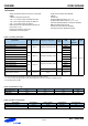
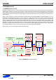
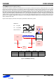
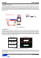
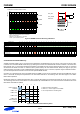
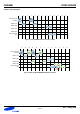
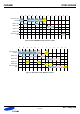
Table Of Contents

Rev. 1.4 May 2009
FBDIMM
DDR2 SDRAM
8 of 42
Figure 5. FBDIMM Command Encoding & SB Frame
Note : The values in “ X” fields in non-reserved commands above may be driven onto the DRAM device pins.
2.5 Southbound Command Delivery
A DRAM command located in the "A" command may be delivered to the DRAM devices as soon as the 14-bit (10-bits in fail-over) CRC
is checked. This minimizes DRAM access latency by allowing the command to be delivered after the first 4 transfers of the frame have
been received. The "A" command is transferred immediately to the DRAM pins with minimum delay whereas the "B" and "C" command
are delivered one DRAM clock later. To minimize memory access latency the read related Activate, Read (if the page is open) and
explicit Precharge commands to a rank of DRAM devices should be placed in the "A" command, if possible. Figure 6 illustrates the deliv-
ery of the three potential commands in a frame to three separate DRAM channels.
Command "A" is delivered in this case to the DRAM devices on DIMM 3 as soon as the command can traverse the AMB buffer. The "B"
and "C" commands are delayed and presented to two other DRAM channels on the following clock. See below figure7~10 for Basic
Read & Write Operations
Northbound consists of 14 differential signal pairs (lane), physically 28 signaling line. Southbound Format has 14x12 (14 IO (or Lane) x
12 IO switching) frame format, which deliver 14x12 bit information per one DRAM clock. One north bound frame is divided into two. Both
frame deliver read data from DRAM
Figure 6. FBDIMM Command Delivery Rules
DRAM Cmnds 23222120191817161514131211109876543210
Activate DS2 DS1 DS0 1 DRAM Addr RS DRAM Bank & Address
Write DS2 DS1 DS0 0 1 1 RS DRAM Bank & Address
Read DS2 DS1 DS0 0 1 0 RS DRAM Bank & Address
Precharge All DS2 DS1 DS0 0 0 1 RSXXXX1 1 1XXXXXXXXXX
Precharge Single DS2 DS1 DS0 0 0 1 RS DRAM Bank 1 1 0XXXXXXXXXX
Auto (CBR) Refresh DS2 DS1 DS0 0 0 1 RSXXXX1 0 1XXXXXXXXXX
Enter Self Refresh DS2 DS1 DS0 0 0 1 RSXXXX1 00XXXXXXXXXX
Exit Self Refresh/
Exit Power Down
DS2 DS1 DS0 0 0 1 RSXXXX0 11XXXXXXXXXX
Enter Power Down DS2 DS1 DS0 0 0 1 RSXXXX010XXXXXXXXXX
reserved XXX001XXXXX0 0XXXXXXXXXXX
Note :
1. aE[0~12] : CRC Checksum of the A Command
2. F[0~1] : Frame Type
3. FE[0~21] : CRC Checksum of 72bit data
4. CRC : Cyclic Redundancy Check
9876543210
0
aE0 aE7 aE8 F0=0 aC20 aC16 aC12 aC8 aC4 aC0
1
aE1 aE6 aE9 F1=0 aC21 aC17 aC13 aC9 aC5 aC1
2
aE2 aE5 aE10 aE13 aC22 aC18 aC14 aC10 aC6 aC2
3
aE3 aE4 aE11 aE12 aC23 aC19 aC15 aC11 aC7 aC3
4
FE21 0 0 0 bC20 bC16 bC12 bC8 bC4 bC0
5
FE20 0 0 0 bC21 bC17 bC13 bC9 bC5 bC1
6
FE19 0 0 0 bC22 bC18 bC14 bC10 bC6 bC2
7
FE18 0 0 0 bC23 bC19 bC15 bC11 bC7 bC3
8
FE17 0 0 0 cC20 cC16 cC12 cC8 cC4 cC0
9
FE16 0 0 0 cC21 cC17 cC13 cC9 cC5 cC1
10
FE15 0 0 0 cC22 cC18 cC14 cC10 cC6 cC2
11
FE14 0 0 0 cC23 cC19 cC15 cC11 cC7 cC3
FE0 FE7 FE11
FE1 FE6 FE10
FE2 FE5 FE9 FE13
FE3 FE4 FE8 FE12
CLK_REF
CLK_DRAM
Packet T/F
12 transfers
x10 bits
A CMD
B CMD
C CMD
Southbound Command Frame Format*
Bit
Transfer
“A”
“B”
“C”
“C”
“A”
“B”
12345
FBD southbound
cmd/data
DIMM 1 cmd
DIMM 2 cmd
DIMM 3 cmd
DIMM 4 cmd
FBD northbound
cmd/data
1. CMD A transferred immediately
2. CMD A, B, C cannot target the same DIMM
3. Host is responsible for scheduling CMD