
User`s manual

S3F80J9 CONTROL REGISTERS
4-3
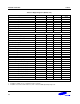
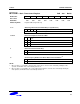
Table4-1. Mapped Registers (Continued)
Register Name Mnemonic Decimal Hex R/W
Port 0 Interrupt Enable Register P0INT 241 F1H R/W
Port 0 Interrupt Pending Register P0PND 242 F2H R/W
Counter A Control Register CACON 243 F3H R/W
Counter A Data Register (High Byte) CADATAH 244 F4H R/W
Counter A Data Register (Low Byte) CADATAL 245 F5H R/W
Timer 1 Counter Register (High Byte) T1CNTH 246 F6H
R
(NOTE)
Timer 1 Counter Register (Low Byte) T1CNTL 247 F7H
R
(NOTE)
Timer 1 Data Register (High Byte) T1DATAH 248 F8H R/W
Timer 1 Data Register (Low Byte) T1DATAL 249 F9H R/W
Timer 1 Control Register T1CON 250 FAH R/W
STOP Control Register STOPCON 251 FBH W
Location FCH is not mapped.
Basic Timer Counter BTCNT 253 FDH
R
(NOTE)
External Memory Timing Register EMT 254 FEH R/W
Interrupt Priority Register IPR 255 FFH R/W
NOTE: You cannot use a read-only register as a destination for the instructions OR, AND, LD, or LDB.
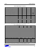
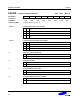
Table 4-2. Mapped Registers (Bank1, Set1)
Register Name Mnemonic Decimal Hex R/W
LVD Control Register LVDCON 224 E0 R/W
Reserved E1H
Reserved E2H
Reserved E3H
Reserved E4H
Reserved E5H
Reserved E6H
Reserved E7H
Reserved E8H
Reserved E9H
Reserved EAH
Reserved EBH
Flash Memory Sector Address Register (High Byte) FMSECH 236 EC R/W
Flash Memory Sector Address Register (Low Byte) FMSECL 237 ED R/W
Flash Memory User Programming Enable Register FMUSR 238 EE R/W
Flash Memory Control Register FMCON 239 EF R/W
Not mapped in address F0H to 0FFH.
NOTE: You cannot use a read-only register as a destination for the instructions OR, AND, LD, or LDB.