
User`s manual

S3F80J9 CONTROL REGISTERS
4-11
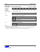
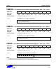
FMSECH — Flash Memory Sector Address Register(High Byte) ECH Set 1 Bank 1
Bit Identifier .7 .6 .5 .4 .3 .2 .1 .0
Reset Value
0 0 0 0 0 0 0 0
Read/Write
R/W R/W R/W R/W R/W R/W R/W R/W
Addressing Mode
Register addressing mode only
.7– .0 Flash Memory Sector Address (High Byte)
Note : The high-byte flash memory sector address pointer value is the higher eight
bits of the 16-bit pointer address.
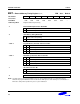
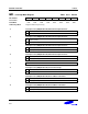
FMSECL — Flash Memory Sector Address Register(Low Byte) EDH Set 1 Bank 1
Bit Identifier .7 .6 .5 .4 .3 .2 .1 .0
Reset Value
0 0 0 0 0 0 0 0
Read/Write
R/W R/W R/W R/W R/W R/W R/W R/W
Addressing Mode
Register addressing mode only
.7– .0 Flash Memory Sector Address (Low Byte)
Note : The low-byte flash memory sector address pointer value is the lower eight bits
of the 16-bit pointer address.
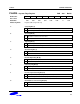
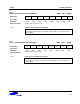
FMUSR — Flash Memory User Programming Enable Register EEH Set 1 Bank 1
Bit Identifier .7 .6 .5 .4 .3 .2 .1 .0
Reset Value 0 0 0 0 0 0 0 0
Read/Write
R/W R/W R/W R/W R/W R/W R/W R/W
Addressing Mode
Register addressing mode only
.7–.0 Flash Memory User Programming Enable Bits
1 0 1 0 0 1 0 1 Enable user programming mode
Other values Disable user programming mode
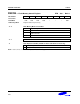
NOTES:
1. To enable flash memory user programming, write 10100101B to FMUSR.
2. To disable flash memory operation, write other value except 10100101B into FMUSR.