SF4300C SERVICE Manual INKJET PRINTER COMPOUND CONTENTS 1. Precaution 2. Referential Information 3. Specifications 4. Disassembly & Assembly 5. Circuit 6. Repair 7. Exploded View 8. Packing 9. Circuit Diagram & Parts List 10. Block Diagram 11. PCB Layout 12.
ELECTRONICS
1. Precautions 1-1 Safeguards Please read these instructions carefully and completely. 1. Do not use this product in a humid place nor outdoor. 2. Do not place this product on an unstable stand or table. The product may fall, causing serious damage to the product. 3. Use this product in a well-ventilated place. 4. Slots are provided for ventilation. Never push objects of any kind into this product through these slots as they may result in a fire or electric shock.
1-3 Static Electricity Precautions Semi-conductors are easily damaged by static electricity. They are usually called electrostatically sensitive devices (ESD). For example, there are IC, FET, and semi-conductor chips. 1) Before you handle semi-conductor parts, be sure to discharge electricity by touching earth connection or putting on a wristband. (Before you turn on the product, put off the wristband to prevent electric shock.
2.
2-2 Location & Outline of Pins of Electrical Parts LOGIC AND CONNECTION DIAGRAMS DIP (TOP VIEW) J SUFFIX CERAMIC CASE 732-03 Vcc E B1 B2 B3 B4 B5 B6 B7 B8 20 19 18 17 16 15 14 13 12 11 20 1 1 2 3 DIR A1 4 5 6 7 8 A2 A3 A4 A5 A6 9 N SUFFIX PLASTIC CASE 738-03 10 A7 A8 GND 20 1 DW SUFFIX SOIC CASE 751D-03 20 1 TO-220 C B . R1=10KΩ . . R2=0.6KΩ . 1 2 3 R1 1. Gate 2. Drain R2 E 3. Source SOT-89 SOT-23 3 1 1 2 2 1. Base 2-2 2. Emitter 3. Collector 3 1. Base 2. Collector 3.
BLOCK DIAGRAM OUT 1 1 IN1(- ) 2 IN1(+ ) 3 GND 4 8 Vcc 7 OUT 2 6 IN2 (- ) 5 IN2 (+) 8 DIP _ + 8 SOP _ + Vcc Q6 Q6 Q12 Q17 Q19 Q2 Q3 IN(-) Q1 Q20 C1 Q18 Q4 R1 R2 IN(+) Q15 Q11 Q10 Q8 OUT Q21 Q14 Q9 Q13 Samsung Electronics 2-3
PIN CONNECTIONS 8 CD FC2 FC1 Vin 1 8 Vo2 2 7 Gnd 3 4 6 Vcc 5 Vo1 1 P SUFFIX PLASTIC PACKAGE CASE 626 (Top View) 8 Block Diagram Simplified Application 1 D SUFFIX PLASTIC PACKAGE CASE 751 (SO-8) Rf 75k Audio Input Cj 0.1 Ri 3.0k 6 Vin 4 _ FC1 3 + Vcc 5 #1 Vo1 Speaker C1 1.0uF C2* 5.
PIN CONFIGURATION (Top Views) KM416C/V10(2)00BJ VCC DQ0 DQ1 DQ2 DQ3 VCC DQ4 DQ5 DQ6 DQ7 N.C N.C W RAS *A11(N.C) *A10(N.C) A0 A1 A2 A3 VCC 1 2 3 4 5 6 7 8 9 10 11 12 13 14 15 16 17 18 19 20 21 42 41 40 39 38 37 36 35 34 33 32 31 30 29 28 27 26 25 24 23 22 TO-92 1 2 3 1.Emitter 2.Base Samsung Electronics 3.Collector KM416C/V10(2)00BT Vss DQ15 DQ14 DQ13 DQ12 Vss DQ11 DQ10 DQ9 DQ8 N.C UCAS UCAS OE A9 A8 A7 A6 A5 A4 Vss Vcc DQ0 DQ1 DQ2 DQ3 Vcc DQ4 DQ5 DQ6 DQ7 N.
OUTPUT B 1 16 SENSE RESISTOR PULSE TIME 2 15 OUTPUT A Vs(B) 3 14 Vs(A) GND 4 13 GND GND 5 12 GND Vss 6 11 REFERENCE INPUT 1 7 10 COMPARATOR INPUT PHASE 8 9 Powerdip 12+2+2 (Plastic Package) ORDER CODE:PBL3717A Powerdip 12+2+2 SO-20 ORDERING NUMBERS: TEA3718SDP TEA3718DP 15 14 13 12 11 10 9 8 7 6 5 4 3 2 1 MULTIWATT-15 ORDERING NUMBERS: TEA3718SFP TEA3718SP (Multiwatt-15) ORDERING NUMBER : TEA3718SP TEA3718DP TEA3718SDP (Powerdip 12+2+2) TEA3718SFP (SO-20) Us DUT B S
nECS2 nECS1 nECS0 VCC6 nWBE1 nWBE0 nWE nOE nCAS1 nCAS0 nRAS1 nRAS0 nRCS2 nRCS1 nRCS0 GND6 ADDR21 ADDR20 ADDR19 ADDR18 ADDR17 ADDR16 ADDR15 ADDR14 VCC5 ADDR13 ADDR12 ADDR11 ADDR10 ADDR9 ADDR8 ADDR7 ADDR6 GND5 ADDR5 ADDR4 ADDR3 ADDR2 ADDR1 ADDR0 1 2 3 4 5 6 7 8 9 10 11 12 13 14 15 16 17 18 19 20 D11 D10 D9 D8 VSS D7 D6 D5 D4 VDD D3 D2 D1 D0 VSS ADDR4 ADDR3 ADDR2 ADDR1 ADDR0 GNDD DCLK SEPWCLK DAOUT GNDD SEPYO GP21 GNDD GP20 GP19 RXDO RLSD GNDD RCVO SWGAINO VCC4 DATA15 DATA14 DATA13 DATA12 DAT
2-3 Chip Replacement (SMD parts) 2-2-1. Precautions for Chip Replacement 1. See to it that the soldering iron does not touch parts directly. In particular, TSOP may be easily damaged by heat. 2. Handle the soldering iron with care and avoid using the same many times. Some parts can be damaged by sudden heat. Preheat parts for minutes at about 100¡c before soldering them. 3. The temperature of the soldering iron should remain at about 240¡c Use a 280¡c iron for bigger parts. 4. Thin (0.
2-2-3 (c) Installation a. Clean the place where a new part will be located. b. Apply water-soluble flux. c. Set a part correctly in place. Prevent it from shifting. d. Stick the part fast without contacting it directly with the soldering iron. Put 0.3mm solder between the iron and the part so that it can melt into the part. e. Check the soldered part with a magnifier. 2-2-4. Chip Tantalum Condenser and Chip Filter 2-2-4 (a) Type There are the following types of chip tantalum condenser and chip filter.
2-2-5 (c) Installation 1. Clean the place where new parts will be installed. 2. Apply water-soluble flux. 3. Locate a part exactly in place. Be careful not to shift it. 4. Stick the part fast with a soldering iron not contacting it directly. Put 0.3mm solder between the iron and the part so that it can melt into the part. 2. Use a ventilation device. a. Choose an injector that suits IC. b. Choose the temperature and the ventilation speed. (normal: temperature - 7, speed - 4) c. Use IC-removing tools. d.
3. Specifications 3-1 Specifications Specification & Features 1. Printer 1-A.
2.
3-1. Facsimile Compatibility ITU-G3 Scan Method CCD Shuttle Scanning Method Scan Width Max. 8.
3-2. Facsimile Feature Gray Scale Use Ext.
Feature Use Ext. Telephone Use PC Tx/Rx Journal No Yes Delayed Dial List No No System Data No Yes Tel Number List No Yes Help List No No Copy Yes (1-Page) Yes (99-Page) Gray Scale No Yes Reduction Copy No Yes Enlargement Copy No No Report & List Print out Copy 4. Electrical & Environment Power Source AC 220~240V, 0.3A, 50~60Hz Dimension (W5D5H) 422(mm) 5 237(mm) 5 180(mm) Weight 3.7kg 5.
4. Disassembly & Assembly 4-1 Taking Off Front Cover This section explains with illustrations how to disassemble the printer. It does not explain how to assemble it, because it is the very reverse of disassembly. Fig.4-1. Taking Off Front Cover -1 ▲ ▲ ▲ ▲ Samsung Electronics ▲ ▲ Disconnect power cords and printer cable from the printer. Unscrew 1 screws on rear cover to separate ink cartridge storage. Push Guide Extension in the direction of the arrow symbol.
4-2 Taking off Rear Cover ▲ ▲ ▲ ▲ ▲ Fig.4-2. Taking Off Rear Cover Push in the paper guide (ÒCÓ) of automatic sheet feeder and place it inside of A4 line. Push the guide manual(L) (ÒDÓ) left. Unhook right and left hooks(ÒAÓ) on the upper part of rear cover. Unhook right and the left hooks of bottom cover by pushing them in. Separate rear cover in the same direction that the automatic sheet feeder is mounted. 4-3 Separating Automatic Sheet Feeder “A” Fig.4-3.
4-4 Separating Main Circuit Board Fig.4-4. Separating Main Circuit Board ▲ ▲▲ Separate various connectors connected with the main board. Separate head cable connected with the main board. Unscrew 3 screws fixed to the main board and separate the main board in the direction of the arrow symbol. 4-5 Separating Power Circuit Board Fig.4-5. Separating Power Circuit Board ▲ ▲ Unscrew 2 screws that fix the right and left ground wire.
4-6. Separating Printer Engine ▲ ▲ Fig.4-6. Separating Printer Engine Remove 2 screws fixed to printer engine unless you unscrewed them at the previous stage. Push outside right and left hooks on the side of the engine, unhook them, and separate the engine in the direction of the arrow symbol. 4-7. Separating Home Assembly ▲ ▲ Fig.4-7. Separating Home Assembly 4-4 Unscrew 1 screw fixed to the back of the engine and separate home assembly from the engine.
4-8. Separating Carrier Assembly Idle Pulley Carrier Shaft ▲ ▲ ▲ Holder Cable ▲ Head Cable ▲ Fig.4-8. Separating Carrier Assembly Separate FPC cable connected with the main board. Separate the holder cable fixed to the main frame. Remove 1 screw on the right of the engine and spring on the left of the engine. Push the left idle pulley in and separate the right part of the timing belt from motor pulley. Pull out carrier shaft and separate carrier Assembly. 4-9.
4-10 Separating Feed Roller Assembly ▲ 1 2 ▲ Feed Roller ▲ Frame Support Bearing Feed (R) ▲ Fig.4-10. Separating Feed Roller Assembly Refer to 4-9 to separate frame base Assembly first. Unscrew 1 screw fixed to the back of the engine and separate frame support from the engine. Turn the bearing feed (R) in the direction of the arrow symbol to separate it from the main frame. Push feed roller on the right to separate it from the main frame.
4-12 Separating Automatic Sheet Feeder ,,,, ,,,, ,,,, ,,,, ,,,, ,,,, ,,,, ,,,, Fig.4-12. Separating Automatic Sheet Feeder ▲▲ ▲ ▲▲▲ Separate the manual plate from frame ASF. Separate the cam pickup on the right and then unscrew the right screw to separate the finger part. Pull out the clutch and then unscrew 1 left screw to separate the clutch part. Separate the guide finger from shaft pickup. Push shaft pickup to the right to separate.
4-13. Separating LIU board Fig.4-13. Separating LIU board ▲▲ ▲▲ Refer to 4-12 to separate automatic sheet feeder from the engine. Separate the connector. Unscrew 2 screws fixed to LIU board. Separate LIU board from the engine in the direction of the arrow symbol.
4-14. Separating Scan Assembly Fig.4-14. Separating Scan Assembly ▲▲ Unscrew 1 screw. Push up scan Assembly in the direction of the arrow symbol to separate it from the carriage. 4-15. Separating White Reference Sheet White Reference Sheet Frame Base Fig.4-15. Separating White Reference Sheet ▲▲ Remove contaminated white reference sheet completely from the frame base. Ask for new white reference sheet.
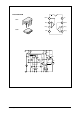
5. CIRCUIT 5-1 MAIN PBA 5-1-1 SUMMARY The main circuit that consists of CPU, MFP controller (built-in RISC processor core: ARM7TDMI) including various I/O device drivers, system memory, scanner, printer, motor driver, PC I/F, and FAX transceiver controls the whole system.
5-1-2 MFP CONTRLLER (KS32C6200 : U15) MFP Controller consists of CPU(ARM7TDMI RISC processor), 2K-byte cache, data and address buses, serial communication part with LIU(Line Interface Unit), print head controller, parallel port interface, external DMA part to receive data from external color image processor (CIPIA:U17), LF/CR motor diver controller and I/O controller. 5-1-2-1. SYSTEM CLOCK The internal clock frequency is 30MHz.
5-1-2-3, LIU(Line Interface Unit) SERIAL COMMUNICATION PART UART (Universal Asynchronous Receiver/Transmitter) at KS32C6200 enables the main and LIU to transmit serial data. The block diagram of UART is as follows: (Fig.5-1-2) KS32C6200 has 2 UART channels. Channel 0(RXD0, TXD0) is used here and the baud rate is 9600bps. TxD 0 TxD 1 IRS UART Block RxD RE 0 RxD 1 IR Tx Encoder IR Rx Decoder Fig.5-1-2.
5-1-2-4 External DMA It brings data from an external device (CIP1A:U17) using DMA channel 0. DMA REQUEST sent from an external device to KS32C6200 activates DMA ACKNOWLEDGE signal and drives DMA channel 0 to produce CHIP SELECT and READ STROBE (/RD) at the external device and bring data from it. It generates address of destination memory, CHIP SELECT and WRITE STROBE (/WR) in order to move this data into destination memory, and then stores the data. MCLK /XDREQ /XDACK D[15:0] /RD /WR Fig.
5-1-2-5. DRAM CONTROLLER As KS32C6200 has DRAM controller in it, DRAM can be connected with external memory. The control mode of DRAM controller enabling EARLY WRITE, NORMAL READ, PAGE MODE, and BYTE/HALF WORD ACCESS supports EDO DRAM as well as normal DRAM. DRAM READ/WRITE signals are /RD and /WR signals used to control system buses. It supports CAS BEFORE RAS for DRAM REFRESH and self-refresh mode for DRAM backup. Connected with common /LCAS, /UCAS and RAS[1:0], it consists of 2 banks.
nSTROBE BUSY PPD(7 : 0) BYTE0 nAUTOFD DATA BYTE BYTE1 COMMAND BYTE Fig.5-1-6 ECP Hardware Handshaking Timing (forward) nACK nAUTOFD PPD(7 : 0) BUSY BYTE0 DATA BYTE BYTE1 COMMAND BYTE nINIT PE Fig.
5-1-2-7. INKJET HEAD CONTROLLER This part produces major control signals used to drive INKJET head. It consists of signals to drive head nozzles, /PHGA[13:1], PHOE[16:1], /FAULT-TEST, /HEAD-EN, and BIASOFF, and consists of signals to check the status of the head, OK 2PRINT and HEAD-DATA. It has double height print head system, 208 nozzles for mono and 192 nozzles for color, and uses /PHGA[13:1], /PHOE[16:1] signals and /HEAD-EN to drive these nozzles. Fig.5-1-8 is timing diagram of each signal.
/HEAD-EN /PHGA1 /PHGA2 /PHGA3 /PHGA4 /PHGA5 /PHGA6 /PHGA7 /PHGA8 /PHGA9 /PHGA10 /PHGA11 /PHGA12 /PHGA13 PHOE1PHOE16 (Tp) Fig.5-1-9. Timing Diagram for Each Nozzle The above control signals are sent to head driver and the head driver converts these signals to the level (+11.75V) to drive head nozzles. 5-1-2-8. MOTOR CONTROLLER (CRPHA, CRPHB, CRIA0, 1, CRIB0, 1, LFPHA, LFPHB, LFIA0, 1, LFIB0, 1) MFP Controller (KS32C6200:U15) supports 2 stepper motors.
5-1-2-9.
PIN NAME CIRCUIT NAME I/O STATE RXD 0 / GIP 0 LIU-RXD I - UART DATA FROM I-LIU CHIP IN LIU RXD 1 / GIP 1 /P-EXIT I H PAPER IS NOT DETECTED L PAPER IS DETECTED /EINT 1 / GIP 2 /MIRQ I H NO INTERRUPT FROM MODEM L INTERRUPT FROM MODEM /EINT 2 / GIP 3 OK2PRINT I H NO FAULT IN PRINTHEAD L FAULT IN PRINTHEAD /EDREQ / GIP 4 /XDREQ I H NO DMA REQUEST FROM CIP L DMA REQUEST FROM CIP UCLK / GIP 5 HEAD-DATA I - CODE DATA FROM PRINTHEAD TCK / GIOP 0 TCK I/O - TEST PIN FOR E
5-1-2-10. RESET CIRCUIT As for SMARTJET there are 2 power resets of primary reset(/F-POR) and secondary reset(/POR) and also reset by watchdog timer (/RSTO). Primary reset is used to initialize flash memory when the system is turned on, while secondary reset is used to initialize the whole system by initializing MFP controller (KS32C6200) after primary reset.
¥ POWER MONITOR (U16: KIA7045F) If +5V supplied to KIA7045F is so unstable as to reach +4.65V - +4.35V (typically 4.5V), it will recognize it as power failure. Then KIA7045F output terminal becomes low (0V) and the voltage is impressed to flash memory and KS32C6200, running RESET (LOW ACTIVE). Flash memory and KS32C6200 are reset first. Thereafter modem, print control parts and CIP(Color Image Processor) linked to /RST-OUT terminal of KS32C6200 are reset as well.
5-1-4 SCANNER 5-1-4-1. SUMMARY This product has CCD(Charge Coupled Device) as an image sensor to receive image input signals and has embodied a shuttle scanner, realizing various scanner control signals and image processing with color image processor CIP1A(U17), which is ASIC for shuttle scan. We are going to look into the principles by explaining the whole data flow in the scanner, block diagram of CIP1A, allocated I/O port and peripheral circuits. 5-1-4-2.
5-1-4-3 CIP1A I/O Port PIN NAME PIN NO.
PIN NAME PIN NO. I/O CIRCUIT NAME GIOP 0 21 O GIOP 1 22 I/O GIOP 2 23 O PRE-HEAT PRINT HEAD PREHEATING GIOP 3 24 I P-EMPTY NO PAPER PAPER READY GIOP 4 25 O /SPK-CTL AUDIO AMP. OFF AUDIO AMP.
5-1-5 PRINTER 5-1-5-1. GENERAL It drives inkjet head to print printing data received from the computer or fax data coming through the line. It roughly consists of head driver, head controller, and the ambient temperature sensor. Fig.6-1-11. Block Diagram of Printer shows the entire structure. 5-1-5-2. HEAD DRIVER (U19, U20, U23, U24) This part drives and inks inkjet head. Color inkjet head drives 192 nozzles, while mono inkjet head drives 208 nozzles. Mono inkjet head is composed of 16 groups of 13 nozzles.
5-1-5-3. HEAD CONTROLLER This part consists of +22V Power Controller to control head driver, Fault Test, Head Detection, Substrate Heating and ambient Temperature Sensor. It checks and controls head driver and ink cartridge. /FAULT-TEST /HGA1 BA1 /HGA13 BA13 KS32C6200 (U15) HOE1 HOE16 BP1 HEAD-DATA Ink Cartridge BP16 (Mono) or (Color) MFP CONTROLLER /FAULT-TEST OK2PRINT /FAULT BIASOFF BS1 HEAD-DATA HSM /HEAD-EN CIP 1A(U17) IMAGE PROCESSOR PRE-HEAT BH1,BH2 THM-DATA THM-CLK Fig.
¥ +22V Power Controller If you insert power cords, the main board will be supplied with power. /POR signal put out through reset circuit activates MFP controller (K32C6200:U15) and MFP controller puts out external circuit reset signal /RST-OUT. This /RST-OUT signal and Vrefx (+2.5V) divided through +30V are impressed to the input terminal of the comparator, putting out +22V if the output of the comparator is ÒhighÓ or getting turned off if ÒlowÓ.
Color Head 70°C No Pre-Heating t Fig.5-1-14. Temperature around Color Head ¥ HEAD DETECTION CIRCUIT Babbage ink cartridge has 8-bit mask ROM I.D. to check the type of cartridge. In order to detect the head, HSM signal is used as ENABLE signal and BA3 signal as START & STOP BIT, and BA1 and BA2 as clock signal of each bit, and ID signal in the cartridge is put in HEAD-DATA port of KS32C6200 through BS1 line. With each bit controlled, 8bit I.D data is read and STOP bit is put out of BA3(LOAD) port.
¥ SURROUNDING TEMPERATURE SENSOR DS1621S(DALLAS SEMI.) is applied to read the temperature around ink cartridge. It is used to get optimum inking quality by keeping the viscosity of ink in the cartridge in the specified lerel. The way to read temperature is similar to EEPROM, controlled by THM-CLK, THM-DATA LINE. Digital thermometer to check the surrounding temperature is assembled along with home sensor in the frame of assembly CR.
HSM BA1 BA2 BA3 BA4 BA5 BA6 BA7 BA8 BA9 BA10 BA11 BA12 BA13 BP1BP16 (Tp) Fig.5-1-17.
5-1-5-5. INK CARTRIDGE ¥ PIN ARRAY OF MONO INK CARTRIDGE There are 208 heater chips in mono ink cartridge.
¥ PIN ARRAY OF COLOR INK CARTRIDGE There are 192 heater chips in mono ink cartridge. One cartridge has 64 Cyan, 64 Magenta, 64 Yellow heaters and (64 x 3 colors) 192 nozzles.
5-1-6 MOTOR DRIVER 5-1-6-1. GENERAL SMARTJET use 2 stepper motors, i.e. CR(Cartridge Return) motor and LF(Line Feed) motor. CR motor moves left and right all-in-one carriage of inkjet head and shuttle scanner. It helps the printer print accurately on the paper and the scanner read image data accurately. LF motor is driven to feed and eject paper for printing and to feed and eject documents to read for scanning.
5-1-6-3. LF(Line Feed) Motor Driving Circuit LF motor is driven to feed and eject documents and paper.
5-1-7 FAX TRANSCEIVER 5-1-7-1. GENERAL This circuit processes transmission signals of modem and between LIU and modem. This circuit is added only to SMARTJET. 5-1-7-2. MODEM (U21) KS16116 is a single chip fax modem. It has functions of DTMF detection and DTMF signal production as well as functions of modem. TX OUT is transmission output port and RX IN is received data input port. /POR signal controlled by MFP controller (U15:KS32C6200) can initialize modem(/RST_OUT) without turning off the system.
5-1-8 OTHERS OPERATOR PANEL DESCRIPTION KEY & LED DESCRIPTION Ready - When power cord is inserted, the system is turned on and initialized. It does not operate but waits for Ready key to be pressed. - If you press the Ready key, the nearby Ready LED will be turned on and the device will be initialized with the system in standby mode. - If the Ready LED is off, the system does not operate though it is on. - Running Print Out Test Pattern Step 1. While Ready LED is off, press ÔReadyÕ key for 0.
5-2 LIU PBA 5-2-1 SUMMARY LIU(Line Interface Unit) circuit added only to SMARTJET is controlled by the main circuit. It monitors telephone line and helps interface between the system and the telephone line. It uses 1LIU(STI9510) to control the whole LIU, MODEM/LINE INTERFACE, RING SIGNAL DETECTOR, DIALER, LINE CURRENT DETECTOR, and SERIAL INTERFACE. 5-2-2 MODEM/LINE INTERFACE This is the path through which transmitted and received data of modem is put in and out.
5-2-5 Line Current Detector ¥ When CML1 relay connects telephone line, U3(STI9510) of LIU board and MFP controller of the main board (U15:KS32C6200) start communication through UART. U3 of LIU board sends signal that includes information of line current value, whenever it receives orders or data from U15 of the main board. 5-2-6 Serial Interface ¥ This part does serial communication with MFP controller of the main board (MAIN PBA:U15) that controls the whole system.
5-3 SMPS 5-3-1 BLOCK DIAGRAM OF POWER CIRCUIT Refer to the following block diagram. AMUNDSEN & SMARTJET POWER SUPPLY (220-240Vac) INLET AC250V2A INPUT FILTER HALF WAVE RECTIFIER FULL WAVE RECTIFIER SNUBBER Nb1 CIRCUIT 3-TERMINAL REGULATOR Ns1 N CH1 +5V RED #1 GND BLACK #2 HALF WAVE RECTIFIER START-UP CIRCUIT SWITCHING DEVICE PWM CONTROL CIRCUIT CH3 +30V GREEN #6 Ns2 HALF WAVE RECTIFIER Nb1 Ns2 VOLTAGE DETECTION CH2 +11.
5-3-2-2. OUTPUT CONDITIONS NO ITEM CH1 CH2 CH3 1 RATED OUTPUT VOLTAGE +5.0V +11.75V +30V 2 RATED OUTPUT CURRENT 0.5A 0.8A 0.5A 3 MAXIMUM LOAD CURRENT 0.8A 1.3A 0.76A 4 LOAD CHANGE RANGE 0.1 ~ 0.8A 0.03 ~ 1.3A 0.05 ~ 0.76A 5-3-3. POWER CIRCUIT 5-3-3-1 INPUT This product is equipped with a three-wire grounding-type power inlet. Insulation is class 1.
5-3-3-4 OCP CIRCUIT (OVER CURRENT PROTECTIVE CIRCUIT) If a short in secondary load terminal or a short inside power device causes excess current, power consumption increases. Then it increases current of power transistor. The current of power transistor increases linearly when it is on. This current is detected by sensing resistance and is impressed to excess voltage protective circuit of PWM control circuit through RC integration circuit where over current protection is built in.
5-4. OTHERS 5-4-1. PAPER SENSING CIRCUIT This circuit senses whether there is paper or not, using photo interrupter. If there is no paper, the lever will cover its sensor and output Ò/P_EXITÓ will become ÒHighÓ. If there is paper, the lever will be lifted and output Ò/P_EXITÓ will become ÒLowÓ. +5V +5V Lever /P_EXIT Photo Interrupter 5-4-2. HOME SENSING CIRCUIT This circuit senses whether carriage is at home or not. This function is carried out when the system is turned on or when the head is capped.
5-4-3 TEMP IC DRIVING CIRCUIT TEMP IC(DC1621S, Thermometer) mounted on the sensor card on the back of the carriage is used to read the temperature around ink cartridge. This IC converts the temperature around IC package into digital and sends the temperature data to serial to make it sense the temperature around the head. It senses temperature so that the temperature of the head can be the optimum when you print something. The above IC sends data serially using signal lines(THM_DATA, THM_CLK).
6. REPAIR 6-1. SCANNER PROBLEM ITEMS TO BE CHECKED HOW TO SOLVE Does the lamp operate normally while shuttle module operates? - Check module lamp. - Check FPC of the main board & module. (J1-1<=> CON2-1: LAMP ON) - Check the path of the main board. (U17[#10]->R185[1K]-Q8->R262->Q7> CON2[#1]) - Replace module. - Replace the main board. Check if white ref. panel is too dirty. - Clean white ref. panel. - Replace white ref. panel. 1.
6-2. SENSOR PROBLEM ITEMS TO BE CHECKED Does the carriage operate normally and go to the initial place, when you turn it on with the carriage placed in the middle? - Check connection between the sensor board of the carriage and the main and check if FPC cable is damaged. - Check if FPC is connected properly with CN1 of the sensor board. - Check if the signal of the sensor is delivered well to CN1-#2 of the sensor board. - Replace FPC cable. - Replace the sensor board.
6-4. PRINTING QUALITY 6-4-1 White lines on letters or graphics. ■ Cause If nozzles in print head has a probkem, white lines are marked on the print. ÔSelf-diagnostic printingÕ will let you know if nozzles have problems. If this line is broken, it confirms that nozzles have problems. ■ Solution 1) Run Ôprint control panelÕ to Òclean cartridgeÓ and check if nozzles have been blocked.
6-4-2 When perpendicular lines are printed crookedly ■ ■ Cause : Perpendicular lines are printed crookedly if you do not Òalign perpendicular linesÓ on the printer. Solution 1) Run print control panel to Òalign perpendicular linesÓ, and 2) Select the best one of the above samples and enter the number. 3) This function to align perpendicular lines is available both for mono and color cartridges.
6-6. Defective Operation PROBLEM ITEMS TO BE CHECKED HOW TO SOLVE 1. No Power? 2. VCC(+5V) ³ +4.5V? 3. U15-130(/POR) is HIGH? (+4.5V or over) 4. U15-153(/RST_OUT) is HIGH? (+4V or over) 1. Check power(SMPS). 1) Cord connection 2) Check each power channel. (+5V, +11.75V, +30V) 2. Check power. 3. Check the circuit around U16. 4. Check data bus of U15. Exchange the main PBA. 1. Check control signal of U15-141 - 145. 2. Check driving output and input signal of U27 and U28. 1.
PROBLEM CanÕt copy CanÕt PRINT In case Defective PC Transmission controls / Reception 1-6 ITEMS TO BE CHECKED HOW TO SOLVE 1. Refer to Ôproblems of scanner.Õ 2. Poor quality of printed image : Print test pattern and check if nozzles have fallen out. 3. CanÕt print.: Check U17-34, 36 signals.(LOW ACTIVE) 1. Refer to Ôproblems of scanner.Õ 2. 1) Check contact between ink cartridge and the head.: Clean it. 2) Check print control signals of U151~10, U15-158 - 160, U15-12~19, and U15-21~28.
PROBLEM ITEMS TO BE CHECKED HOW TO SOLVE 1. Check CON3(main PBA), main LIU harness, and P1(LIU PBA). 2. Output of U2-4(LIU PBA) is HIGH? (+4V or over) 3. Refer to 3,4,5 and 6 of ÔDefective Transmission/ReceptionÕ in ÔIn case PC controlsÕ. 1. Replace defective parts. 2. If high, check the surrounding circuit and replace LIU PBA. 3. Refer to 3,4,5 and 6 of ÔDefective Transmission/ReceptionÕ in ÔIn case PC controlsÕ. Automatic Reception Failure 1.
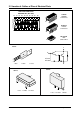
7. Exploded View 7-1.
Availability of Materials Minimum Q’ty MEA-BRKT LF1 : MJ-705G/MJ-705A MEC-BRKT LF : MJ-705G/MJ-705A BRKT-LF MOTOR : SECC T1.2 GEAR-LF IDLE1 : POM GEAR-LF IDLE2 : POM GEAR-LF IDLE3 : POM GEAR-LF IDLE4 : POM BEARING-FEED L : POM MOTOR-STEP(LF) : NMB MOTOR O O ✕ ✕ ✕ ✕ ✕ ✕ O 1 1 1 1 1 1 1 1 1 JB75-10938A JB70-10908A JB70-10909A JB70-10910A MEC-FRAME MAIN : MJ-850S/MJ-860X IPR-FRAME MAIN : SECC T1.2 IPR-RAIL CR 2 : SECC T0.8 IPR-SUPPORT BASE : SECC T1.
Availability of Materials Minimum Q’ty PMO-LEVER FINGER : ACETAL (NA) SPRING-FINGER LEVER : SUS 304 WPB IPR-BRACKET FINGER : SECC T0.
Location Code G1 G2 G3 0205-001002 0205-001007 961 171005AB 7-4 Part Name & Specifications GREASE : NYOGEL 744 GREASE : NYOGEL 759G GREASE : CRS841 Availability of Materials Minimum Q’ty O O O 1 1 1 Samsung Electronics
Samsung Electronics S8 212 205 204 107 106 206 202 201 108 207 203 G2 208 210 104 211 209 1103 105 103 200 608 S1 607 601 101 1101 102 G1 S4 100 603 503 604 605 606 602 600 501 S4 502 315 311 305 307 312 1104 306 314 313 308 504 550 301 500 1902 1901 310 800 305 303 304 309 G3 1700 1900 1803 1802 305 302 701 1200 1804 1801 G4 405 404 302 S9 1804 S7 406 S5 1102 401 402 409 407 408 702 2200 S3 700 S1 902 901 1106 903
4 7 Samsung Electronics IEW TV ON FR 5 3 2 4 4 6 5 6 7 CODE NO JB69-20904A JB69-10930A JB69-10932A JB69- 30901A JB98-00918A JB98-00922A MEC-CARRIER SHEET JB75-10986A JB68-10208A LABEL(P)-BARCODE MEC-GUIDER BANNER JB75-10944A BOX-MAIN(MJ-850S) BOX-MAIN(MJ-860X) BAG-SET 4 INA-ACCESSORY 3 2 1 CUSHION-L/R NO HDPE T0.015X700X600 MJ-850S MJ-860X PE+SC400 ART PAPER HIPS DESCRIPTION EPS 60M SW-3 WHITE(OFFSET UV) SW-3 WHITE(OFFSET UV) 1 1 1 1 1 1 1 1 Q'TY 8.
9. Electrical Parts Lists MAIN B’D P/L No. SEC CODE DESCRIPTION PART NAME VENDOR Q’TY Location 1 0401-001003 DIODE-REC,MMBD6050LT1,0.2A,70V MMBD6050LT1 MOT 2 D3,D4 2 0402-000199 DIODE-REC,100V,1A,DO-213AB EGL41B GI 1 D2 3 0403-000284 DIODE-ZENER,MMBZ5237B,8.
No. SEC CODE VENDOR Q’TY 32 2007-000026 R-CHIP, 200ohm,5%,1/10W RC2012J201CS SEM,ROHMK 5 33 2007-000028 R-CHIP, 39ohm,5%,1/10W RC2012J390CS SEM,ROHMK 19 R215,R63-R66, R69,R301-R313 34 2007-000029 R-CHIP, 0ohm,5%,1/10W RC2012J000CS SEM,ROHMK 1 R29 35 2007-000221 R-CHIP, 0ohm,5%,1/10W RC2012JOOOCS SEM,ROHMK 3 R362,R363,R353 36 2007-000223 R-CHIP, 1.2Kohm,5%,1/10W RC2012J122CS SEM,ROHMK 1 R368 37 2007-000238 R-CHIP, 1.
No. SEC CODE DESCRIPTION 65 2007-000710 R-CHIP, 6.8Kohm,5%,1/10W 66 2007-000757 67 VENDOR Q’TY RC2012J682CS SEM,ROHMK 1 R265 R-CHIP, 330Kohm,5%,1/10W RC2012J334CS SEM,ROHMK 1 R251 2007-000766 R-CHIP, 300ohm,5%,1/10W RC2012J331CS SEM,ROHMK- 2 R211,R212 68 2007-000814 R-CHIP, 39.
No.
No.
No.
LIU B’D P/L No. SEC CODE DESCRIPTION 1 0401-000140 DIODE-SWITCHING, 1N4148, 100V, 200mA, 500mW, 4nS, DO 2 0402-000339 3 VENDOR Q’TY IN4148T/R DSMS, NSC, TERRY 2 D1,D8 DIODE-BRIDGE, W06F, 600V, 1.5A W06G GI 1 BD1 0403-000139 DIODE-ZENER, 1N4734A, 5.
No. SEC CODE DESCRIPTION 34 2007-000757 REF-CHIP, 330K, 5%, 1/10W, 150V 35 2007-000774 36 VENDOR Q’TY RC2012J334BS SEM, ROHMK 1 R10, 21, 23, 32 REF-CHIP, 33Kohm, 5%, 1/10W, 2012 RC2012J333CS SEM, ROHMK 1 R41 2007-000931 REF-CHIP, 470, 5%, 1/10W RC2012J471CS SEM, ROHMK 1 R44 37 2007-001001 REF-CHIP, 510, 5%, 1/10W RC2012J511BS SEM, ROHMK 1 R39 38 2007-001071 REF-CHIP, 6.8K, 5%, 1/10W, 150V RC3216J682CS SEM, ROHMK 1 R2 39 2007-001141 REF-CHIP, 7.
SCAN B’D P/L No. SEC CODE DESCRIPTION 1 2007-000703 R-CHIP,3.6Kohm,5%,1/10W RC2012J362CS SEM,ROHMK 1 R1 2 2007-000868 R-CHIP,4.7Kohm,1%,1/10W RC2012F4701CS SEM,ROHMK 2 R3,R4 3 2007-001013 R-CHIP,51ohm,5%,1/10W RC2012J510CS SEM,ROHMK 1 R5 4 2007-000518 R-CHIP,2.
LAMP B’D P/L No.
SENSOR B’D P/L No. SEC CODE DESCRIPTION 1 0604-001045 PHOTO-INTERRUPTER,TR,0.
SMPS B’D P/L No. 1001 ITEM IC-SHUNT REG 1001-A 1002 IC-REGULATOR DIODE-SWITCHING DIODE-SCHOTTKY DIODE-F.R 1005-A 1006 DIODE-ZENER 5V 1A 1N4148 DIODE-ZENER 75V 0.15A 1008-A SAMSUNG ROHM KOREA 1N5822 40V 2.5A MICRO SEMI D3S6M 60V 2.5A SHINDENGEN SF34 200V 3A MICRO SEMI MTZ20C MTZ6.2C TZP15B 1 U1 1 U2 1 D1 1 D2 2 D3, 4 1 ZD1 1 ZD2 1 ZD3 UNIZON SHINDENGEN 0.5W 20V ROHM KOREA UNIZON 0.5W 6.2V UZ6.
No. 2003 ITEM CAP-Y 2003-A 2004 CAP-ELEC CAP-ELEC CAP-ELEC CAP-ELEC CAP-ELEC CAP-ELEC CAP-ELEC CAP-CERAMIC CAP-CERAMIC CAP-CERAMIC CAP-MYLAR CAP-MYLAR 2015-A 2016 25V 560uF 10*25 SRE50V1uF SMS50V22uF CKR3A471KO6BS CKR3A101K06BS CCYV1H104ZF CAP-M.F 50V 1uF 3.
No. ITEM PART No. DESCRIPTION VENDOR 3002 R-METAL 1/2W 560K-J NORMAL TYPE L:9mm ABCO 3002-A R-M.O 1W 560K-J MINI PILKOR ABCO 3003 R-METAL OXIDE 1W 330K-J MINI PHILKOR 3003-A 3004 R-METAL OXIDE 1W 47-J MINI PHILKOR R-METAL OXIDE 1W 470-J MINI PHILKOR R-METAL PHILKOR 1/8W 100-J R-METAL PHILKOR 1/8W 47K-J R-METAL OXIDE 1W 1.0-J MINI PHILKOR R-METAL PHILKOR 1/8W 330-J R-METAL PHILKOR 1/4W 390-J R-METAL OXIDE 1W 110-J MINI PHILKOR R-METAL 1/8W 4.
No. 4002 ITEM SURGE ABSORBER 4002-A 4003 BEAD CORE 4003-A 4004 BEAD CORE 4004-A PART No. DESCRIPTION VENDOR JVR14N471K UL JOYIN SVC471D-14A SAMHWA BFD3550R2F SAMHWA RTD3550S(R2) NAMYANG BFS3550R2F SAMHWA RTS3550S(R1) NAMYANG Q’TY LOCATION 1 TNR1 1 B1 2 B2, B4 4005 BEAD CORE F-FB35T 3.
No. 4016 ITEM PCB PART No. IFPS-V2 DESCRIPTION FR-1 1.6T VENDOR CHUNG JU Q’TY LOCATION 1 GANA 4016-A 4017 LABEL IFPS-V2 SAMSUNG PRINTEC 1 4018 SCREW-FG MSBH 4*6 SCREW+WASHER DAEKYUNG 1 4019 SCREW MSBH 3*6 TAPTITE GLD DAEKYUNG 4 4020 SCREW MSBH 3*10 GLD DAEKYUNG 2 J1~J4, J6~J9 4021 WIRE JUMPER 0.6mm SAMEUN 8 Q1, 2 4022 SILICON RUBBER TUBE 9.5*27 0.45T MUNG SUNG 2 CAP TO-220 0.45T APEX 4022-A 4023 CLAMP-TR4 DONG IL SPCC 1.
Samsung Electronics 3000PI CCD (COLOR or MONO) CCD MODULE DOUBLE HEIGHT 6000PI PRINT HEAD KEYS & LEDS CCD MODULE INTERFACE PART CHECK 7 PREHEAT PRINT HEAD (8BIT*2,7BIT*2) PRINT HEAD DRIVER LINE FEED MOTOR DRIVER LINE FEED MOTOR PAPER EXIT SENSOR CARRIER MOTOR DRIVE CENTRONICS CABLE CARRIER MOTOR PERSONAL COMPUTER PARALLEL PORT INTERFACE PART MAIN 9600bps MODEM* DMA I/O PORT SCAN CNTR I P 8BIT ADC CIP 1 (30MHz CLK) DMA 3 INT.
Samsung Electronics CR MOTOR PRINT HEAD Modular Jack SCANNER Ext.Tel Line Liu B'D SMPS Main B'D ASF Paper Empty Sensor SPEAKER LF MOTOR 11.