SHARP SERVICE MANUAL CODE: OOZMZ8OOIIIIE PERSONAL COMPUTER MODEL MZ-800 MZ-1P16 MZ-1E20 Table of contents t, 2. 3. Specification .. Parts identification .. Systemdiegram .. . .................................... 4 4. Systemdescriplion .. 4·', Memorymep .. ................................................... 6 .. 9 4-2. CustomLSI ..... 4-2-1. Memoryconlroller ... 4-2-2. 4-2-3. 4-2-4. 4-2-5. VOcontroller .. Clock generator end timing generator .. Display address generator ...
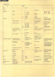
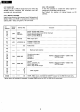
1 SpedfIution -f- t IMl-700 - "'ItB W.fJOO - 8ItB CG I;:' - :::.... Dicpl'vmethod .CoIor 8'lm.p ..... thod - Resolution PCGmalhocl ... ,,.. 320 >e 200 OP 320 >e 2OO ~~ >e 2OO Colo< ..slgn .......1 Se'Mn.ndchl.KtIt Se.Mn ~h'ndling ~_Ienc:oc* M!~7~moo.only ~- '''''''' 10<121 10<121 180< '''', c:oIora ~0:010010 900'.ochltac:t... ~••• glnl"'ed- ---- ~of18co1ort; _I--- - "'1t8 ...,. "'coIofl ChOHn out of 1ScaIO,. ~......tlon _+---+==",-~__ ~keOfI8caIO" Cen"onlclinterl_ =:!.
~ilZ-800 2.
MZ-800 3. System diagram MZ-1A18 AAMfile MZ-1A25 Expansion RAM MZ-1x17 MZ-1E19 MZ interface MZ-1E20 MZ-1U06 1U06 interfacing PWB Expansion VO box MZ·1F11 MZ-6F03 MZ driver MZ blank media MZ-2Z046 DISK BASIC MZ-1P16 MZ-2Z047 Plot printer CP/M MZ-1D04 12", 8-tone, monochrome CAT MZ-1D19 14", 18-color, AGBI, CAT /I~ 0, 'J).
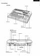
MZ-800 4. System description 16 KB l Basic RAM, 64KB r---' I I l. r- L _~ PPI 8255 -, MZ-1P16 --- Plot printer l OP I ,.--J KEY PlO Z-80 PlO CMT VF MlSOP5K printer Printer interface CTC 8253 r----+----.J Joystick interface (ATARI compatible) PSG RGBI SN76489 CRTC AMP (Semi-cuslom) MZ-1D19 o VRAM 16 KB rI I --, MZ-1R18 slol (dedicated) I I r - -----, I Expansion slot-l I L L ___ -.
CJ1 1 OSCJ Cursor 556 Z-80A GDG ·1 t... LJ [ 1 WE &J 8253 DATA RECORDER AMP II~~ ~ lci7Jt PC21 ~rl CTC Peripheral VO bus CAS RAS CSROiI.1 I- Option 16 KB dn' ~ --c= CONTROL BUS DATA BUS VRAS OSC 556 VRAM DATA BUS RESET VRAM ADR. BUS ADDRESS BUS ~CustomlC t I~ cPU~ 0= 3.547 MHz RGBI 00 u 0" u., ~~~ '17.73 MHz -~ Monitor, SP L--+_ _ _, PA4 PA5 r PAf PBI Z-80A PlO T 16KBROM (27128 'I1L/"""'I L\2- fi 1"" w c. )( 0 ." 'Cij " ~ £ I ~ ..
MZ-800 4-1. Memory map The MZ-800 has a different memory map depending on the mode. To have compatibility with the MZ-700, it has two modes of the MZ-700 mode and MZ-800 mode. o MZ-800 memory map MZ-800 mode MZ-700 mode FFFF" EOOO ~ ~ 0000 COOO O[J D AOOO 01000 -- MAIN MAIN o-RAM o-RAM 64K. 64 KB I I : : ~ __ J OVOR"';: __ , ,.--, 1 I I I I n : lml: 1: IIV) II L__ J 1 II 1 L __ oJ ~ 640 )( 200 mode 320 x 200 mode 4000 NOTE: ,- __ .J Item within dotted lin.
MZ-800 Memory Sank Control ~ port MODE Function SEO SEl - SE2 - MZ-SOO mode MZ-7oo mode SE3 MZ-7oo mode SE4 MZ-SOO mode MZ-7oo mode MZ-800 mode o SOOOO - S7FFF o Soooo - SFFFF o SEooo - SFFFF o SOOOO - $OFFF o $0000 - SFFFF o SEooo - SFFFF o SOOOO - $OFFF o SOOOO - $OFFF to DRAM. to DRAM. to DRAM. to monitor to VRAM, key monitor monitor monitor to to to ROM. timer, and ROM. ROM. ROM. monitor ROM. o Slooo - $CFFF o Slooo - SlFFF to DRAM to CG ROM.
MZ-800 ~rt MZ-700 mode MODE Function 0000 1000 MZ-800 mode MZ-700 mode IN (SEO) MZ-800 mode MZ-700 mode r--l I--l 1--' 1--, ,---, I I I I I I I I I I I I 3000 4000 5000 8000 I I I I MZ-800 mode MZ-700 mode 9000 Aooo I I I I I I I I I I MZ-800 mode I 1 I 1 I I 1 1 I I I I I I I I I I I I I I I I I DRAM (NOTE) I I DOOO 1 I Eooo State before prohibited Prohibited I I I I I ---- V RAM (CGRAM) Prohibited I V RAM I I I 1 I B B I I I r--, I I I I
MZ-800 4-2-2. 1/0 controller In this I/O controller is created the select signal for assignment of MZ-800 internal device. See Table-2 for relation of internal device vs I/O address. 4-2. Custom LSI The custom LSI is a 100-pin single chip LSI on which the MZ-800 memory controller (I/O controller) and CRT controller, etc. are contained. 4-2-1. Memory controller Used for the control of the memory bank.
MZ-800 Pin No. 1 2 3 4 Signal name 1/0 CPU 5V GND ADO - I I 19 20 ADF DTO I I on 27 28 -----0--29 --30 GND VCC MREO -- RD 31 WR 32 RFSH 33 IORQ 34 e----,.;----- I--Ml 35 ---36- -SEL1 CASB 37 INH5 ~8 f-----VBLN 39 1-- 40 GND 41 VRAS 42 IJCli:S 43 VADO I _._--50 51 52 53 54 55 Functional description 0 CPU clock (3.
I MZ-800 Pin conflgur.tlon m TlM' C&3 ~G CKMS JOY IIOIIT IIISTO CI"$ IOWR TEST KEY CIJR MOO MNIfT SIC lORD MOO' Mm CJIIOM ..... GNO GNO ADO ...... AOl ~TN AD' G"N BlUE •• 0 sac. ... AD7 VC> AOO vet; AOA \IC4 VCI ADO VC, ADC VC2 AOO VC. AD' VA7 \/CO OTO VAB on VAS 072 VM 073 VA3 0" 0" VA2 VA1 .....
MZ-800 4-2-4. Display address generator 1) Display address generation • Display address increments from left to right as beginning from the home position at the upper left corner of the CRT screen (address $000). The first display line dominates address $000 through $027.
I MZ-800 4) Line scroll SOF = $O~ $28 Programming "SOF = $28" makes the display screen shifted eight lines up. Data on the highest line therefore shifted to the bottom line. Programming "$28 ~ $0" makes the display screen shifted eight lines down, and the line on the bottom moves to the highest line. 4-2-5. Scroll 1) Scrolling is possible for both horizontal and vertical directions by means of software offset. The following four registers are use~ for scroll control. a.
MZ-800 Scroll control register SSA: Scroll start address Increment of SSA: $5 Minimum value of SSA: $0 Maximum value of SSA: $78 Scroll and and control circuit hardware • Block diagram Scroll offset Scroll width Start address MSB LSB N 6 3 4 5 2 SEA: Scroll end address Increment of SEA: $5 Minimum value of SEA: $5 Maximum value of SEA: $70 SOF LSB MSB N c SEA-SOF 10 DA(MA) 5 3 4 2 SW: Scroll width Increment of SW: $5 Minimum value of SW: $5 Maximum value of SW: $70 Relation of SW. SEA.
MZ-800 Concept of the scroll control circuit Scroll method • Scrolling by means of VRAM address conversion. Execution of scrolling by address conversion • Scroll offset (SOF) is the count of lines which the CPU gives to the CRTC. For instance, the following must be observed to perform scrolling. 3-line scroll: SOF3 = OF x 3 5-line scroll: SOF5 = OF x 5 And, to scroll one more line after 5-line scroll; 5-line scroll: SOF5' = SOF5 + OF = OF x 6 Range of scroll • y-axis programmable.
MZ-800 • Read For plane read data from the VRAM, data to be read by the CPU are arranged in accordance with the direction of the read format register (RF). As the PCG method is adopted for the MZ-700 mode, the text and ATB areas are actually mapped to $0000 - $OFFF. So, the VRAM address has the following relation with the display character position. 1 2 3 40 :1:: 1 1-1 0001 11"'0 -1 ~".n. t. 11 ) •.
MZ-800 MZ-700 MODE DISPLAY TIMING 56.3ns r=: ClK 451ns ... 1 ,'---- ~--------------~, VRAS VCAS VOE , ''-_----'I ~ VAD 0-7 X X'---'-'-'-''--''-'-----' ATB. adr. X 'ROW X COL. X DUMMY adr. • X X ---v----' '----------' __ ROW COL. '-----v-----' ~ -.J ' - - - - CG. adr. text adr. ------- --~C=>>---->-------->------>----- VAO -7 ' lOAD (shift register) text DATA CG.DATA ATB. DATA invalid DATA , ...._ - - - .... -----' MZ-SOO MODE (320 X 200 dot) ClK \ VRAS .
MZ-800 1) 320 x 200 dots See the figure below for VRAM configuration and CRT character display position.
MZ-800 800 MODE (640 X 200 dot) DISP. cycle -I· ,'---___----~I VRAS VA 0 - 7 0 - 7 ~ ROW X'____CO_L_.----'X'____C_O_L._~'C~'___ _ _ _ _ __:_--~X '---;;~ '------C~ N+1th adr. I plane N+l th DATA X'-__--,--_ ~===N=+=-2th~ad-r.~~ cPU read DATA ----------~~~----~~~----~<==>~---------------~ III plane Nth DATA 1II plane N+ 1th DATA CPU read DATA LJ CPU and VRAM accessing 1.
MZ-800 4-2-7. Register functions VRAM configuration • One or two chips of 16 KB VRAM are used. • In the case of a single 16 KB VRAM chip, it handles 320 x 200 dots, 4 colors, or 640 x 200 dots 1 color. • In the case of two 16 KB VRAM chips, it handles 320 x 200 dots, 16 colors, 640 x 200 dots, 4 colors, 320 x 200 dots, 4 colors, 2 frames, or 640 x 200 dots, 1 color, two frames. • DMD 3, 2: Display method and resolution DMD 2 3 o o I o 1 -----~-- -i next are about functions of the custom LSI.
MZ-800 VRAM to CPU interface • SRCH/S I NG "0": Single color data read ..... Reads the data of the color plane, 1, IT, rn, or N, specified by "1 ". NOTE: Only one item should be "1" out of I, IT, rn, and N. If it is "1" for more than two or non-existence of the VRAM may not assure the data read. "1": Specified color search ..... "1" is retu rned for the bit of the color specified by 0/1 of I, IT, rn, and N.
MZ-800 Table-2 Display mode vs read format register Display mode SRCH/SING B/A IV m n Function (NOTE) --------------r---------------+--------+---------~----~----_+----_r----~--------------------__i 320 x 200. 4116 colors Single color data read Frame A: "0" o o o o o Plane I data read o n data Plane read ~--~-----+-----+----~----------------------- Frame B: "1" 640 x 200.
MZ-800 b) Write format register (WR) (OUT & CC) • WMD 0 - 2 ..... Selects the logical operational mode for readmodify-write . • • rn, I, Il, IV ..... Color plane designation Write mode '2 -SINGLE-- . +- 0 WRITE WMD 1 0 0 0 1 o r --tr0- EXOR ----t-- - OR o I __ RESET 0-1 ~ 1- B/",: IV 0/1 (*) ~ Frame A: 0 11 ---j 01 Frame Color plane ill IT -~ Function 0/1- I o~T, ~/~ +,1,'~/01, ,-- t---r- OIl I --;1 B: 1:_~/~ .
MZ-800 CD REPLACE c) Example of CPU read/write access • Shown next are access examples of REPLACE write, PS ET write, and SEARCH read in the 320 x 200, 16-color mode. As for display colors, Plane I corresponds to 8, IT to R, ill to G, and IV to I. write • To develop light yellow characters on the graphic screen.
MZ-800 (FO H ) 4-2-8. Pallet • As there are four 4-bit pallet registers provided inside the unit, it permits choice of R, G, B, and I combinations, and it enables to make choice of any desired two or four colors out of sixteen available colors. However, in the 320 x 200, 16-color mode, choice of colors permitted to four kinds of colors output of sixteen. • Only the conventional mode is applicable for the MZ-700 mode without using pallet.
MZ-800 (Ex.) c. e'" Cl An example of the pallet in use in the 320 x 200, 16-color mode • Assume that the pallet register has been set to the following. PLTO = Black PLT1 = Cyan PLT2 = Red PLT3 = Magenta • When SWo is set to "0" and SW, to "0", the pallet is applied to four colors in group 1 (ill = 0, N = 0) and it results in the color as shown in CD of the table right (yellow to cyan).
MZ-800 4-2-10. ROM configuration The MZ-700 monitor, character generator (eG), MZ-800 monitor, and IPL are implemented on a single chip of 16k x 8-bit ROM. ROM add.... soooo Mapping address ,..-------. $0000 MZ-700 monitor $1000 ~----~ $1000 CG Not used $2000 $Eooo $E010 QD-IOCS FD $3000 $ESOO (start address) MZ-800 IPL & monitor IPL & monitor QD command $F400 $3FFF BASIC 10CS Version pending on the mode.
MZ-800 8255 From keyboard PBO Key data input pin (a-p) I 07 PB7 07 I I DO DO VBlNK PC7 556 OUT PC6 Al Al PC2 AO AO READ PC5 MOTOR PC4 RD PC3 MOTOR ON WR PCl WRITE PCO KEY To keyboard PA7 PA3 Key data strobe (10-p) RESET 55 RESET PA2 lS 145 PAl PAO LS145 decoder, and PSD-PS7 are connected to the key matrix directly.
MZ-800 Key strobe is issued through PAo-PAl to ~can the key. As it is supplied to the decoder, it makes one of outputs, 0-9, set low. It is then added to the key matrix to scan the line of the key depressed (vertical key matrix scan). The line is in the low state, if it is in depression (horizontal key matrix scan). NOTE: In the ready for command state, PAo-PAl are normally repeats to be low state and the decoder outputs repeats to be high state.
MZ-800 See next for the contents of the information block. Byte count Name Function Note ATRB 1 Attribute NAME 17 File name (16 characters maximum) CR (OD) affixed SIZE 2 File byte size In order of low to high order DTADR 2 Loading address EXADR 2 Execution address 1---- 104 COMNT Comment Not used Rotation of the cassette (dedicated) is controlled by the 8255 and its peripheral circuits.
MZ-800 4-4. 8253 Programmable Interval Timer The 8253 makes sound generated with the counter #0 and internal timer is operated with the counters #1 and #2. • Counter mode #0 ..... Square waveform generator MODE3 #1 ..... Rate generator MODE2 #2 ..... Interrupt on terminal counter Ao Do D, D, Data bus A, A, Aa 1r 8! A. As Ds Ds D7 7 BlA CID PlO control GE.
MZ-800 Signal name Description Pin No. I/O 19,20,1 40,39,38 3,2 1/0 Z80-CPU Data Bus Bidirectional, 3-state, Z-80 CPU bus. Data and command transfer between the Z-80 CPU and the PlO is carried out through this data bus. Do is the least significant digit. B/A 6 I Port B or A Select Port select signal. Depending on the state of this signal, the port is specified through which data or command is transferred between the Z-80 CPU and the PlO.
MZ-800 Pin No. 1/0 23 0 Interrupt Request Connection with CPU INT signal. A low on this line causes the PlO to place an interrupt request to the CPU. Because it is of an open drain type, it is possible to make INT of several peripheral LSI wired OR using the pullup resistance. Ao-A, 15-12 10- 7 1/0 Port A Bus Port A data bus. Data transfer is carried out with the PlO and peripheral device via this bus. AD is the least significant digit.
MZ-800 Pin name 1/0 Active Signal name PAD PA, PA2 PA3 PA. PA5 PAs PA, IN IN IN IN IN IN OUT OUT L L - RDA STA GND GND PB. PB, PB2 PB3 PB. PB5 PB. PB, OUT OUT OUT OUT OUT OUT OUT OUT W u. ~ <{ t: e a.. LL U. ~ co t: e a.. H H H H - A low on this line indicates that the printer data is ready to receive. A low on this line informs the personal a paper depletion during status check. An 8253 output used for interrupt. Horizontal blanking signal used for interrupt.
MZ-800 4-7. Joystick It permits connection of two ATARI compatible joysticks. ADO JOY ~ ,l Gl 1---, G2 ,.. FWD DT0 I ~--I---. 1 I ~ ! BACK "3 LEFT 4' DT 1 -<1- DT 2 DT 3 SW '-------~~~--~I~ RIGHT 6 ,.. DT4 '7 DT 5 2SW type only TRG2 Configuration of ATARI compatible joystick I >>-_____....,I't-.. V PA4 4tWM 4-8. System switch setup System switches are assigned as follows: + 5V ~GND SW No.
MZ-800
MZ-800 2. INSTALLATION (Fixing the printer) 1. Fix the printer unit on the table as shown in the figure. (Place the printer in the arrow direction (D, lightly move in the arrow direction S, then secure it with screws.) ~/ * It is also possible to use the printer free on the table without securing. / r= =======lI Screw for securing the printer ~ Connection procedure after the installation (D Make sure that power is off to the MZ-800 and its peripheral units.
MZ-800 3. OPERATION 3-1. Block diagram H \ ,j H Connector r-- I-- ~ V-axis stepping I-motor J. Drive array I I-- interfacing Buffer I--- , Intelligent - ,--- \ \ I-- ~ X-axis stepping motor ~ Pen up! down magnet , J LSI ~ 1\ , Magnet drive circu it ........ ,. , L_ ,... I _J Printer mechan ism Control switches {paper feed Reset Pen exchange 3-1-1.
MZ-800 3-2. Pen exchange method It is more effective to save power to shut off current while the X and Y axis motors are at a halt. But, there may be a possible malfuction because of unsuppressed vibration, if the current is turned off with a normal pulse width. In order to prevent this, current is applied excessively for more than the given hold time (tMH = lms or more). To remove pen, press the pen exchange button, when the slider is at the right handside, push the pen release lever. Motor 3-4.
MZ-800 3-6. Colour plotter printer control LSI Pin assignment Name Symbol Function In/out Vss Ground Connected to OY. Vcc Main power Connected to 5Y. Voo Power Connected to 5Y. PROG Program Plo ~P17 P2 0 ~ P27 Do - D7 I 1 I To Tl I Not used. Out Port I Used as printer control signals. Port 2 Used for data input port from CPU. Data bus Used for stepper motor control signals. Test pin 0 In Test pin 1 In 1 Input from pen change switch. I Input from paper feed switch.
· ,vIZ-800 3·7. Interfacing with the MZ·800 Fig. 1 shows the block diagram for connection with the printer. Fig. 2 shows its circuit description. Fig. 3 shows the timing chart.
MZ-800 4. COlOR PLOTTER-PRINTER CONTROL CODES 4-1. Control codes used in the text mode • Text code ($01) Places the printer in the text mode. • Graphic code ($02) ................................................ Same as the BASIC PMOOE statement. Places the printer in the graphics mode. • Line up ($03) .......................................................... Same as the BASIC PSKIP statement. Moves the paper one line in the reverse direction. The line counter is decremented by 1. • Pen test ($04) .......
MZ-800 4-3. Graphic mode commands 4-3-1. Command type In the graphics mode, the computer can control the printer with the following commands. The words in parentheses are BASIC statements which have the same functions as the graphics mode commands. Command name LINE TYPE Format Lp (p=O to 15) ALL INITIALIZE HOME (PHONE) A H INITIALIZE (HSET) I DRAW (LINE) Dx, y, ... , xn, yn (- 999~x, y~999) RE LATIVE DRAW (RLINE) J.:lx, .:ly, ... , .:lxn, .:lyn ( - 999 ~ .:lx, .
MZ-800 1 2 3 4 5 , MZ-800 7 • • 10 n 12 CPU P.W.B.
MZ-800 2 3 Cassette Recorder Caution of the Assembling • Be sure ® and ® must be in exact position. Otherwise tape data will be destroyed when "play" is done.
MZ-800 10 9 8 7 11 12 Cassette Recorder Circuit • ,r------- ---------- -- ----- ----------------- -- -----·---· , "," Ht., J , B . , ." '[ ' 0 c ,, ,, , ,, I I Cl , L __________ _____ _ ____ _________________ __ ___ __ _ _______ J "' - ~ . TotIO"' """O.•..... M,., . ,,, _____ ~"" ,~''''O. ~J'( ' ''OO< "CO" "'", al.' _____ ,,,"'.......,.., { o '.U ____ '''''"'' G", ". "" ",.'RHV ....Q.f·' ." ". ''' '1C~ ' ''' ,"". O"Ee' ",,,,,"'" -----l:.- .",,".," ,.
MZ-800 I I 1 3 2 I I 4 5 6 MZ-1P16 CIRCUIT " - c .. z ( ..
-800 MZ-800 , 1 9 10 " 12 MZ-1E20 LAYOUT • , • , , , , c o JOY STICK LAYOUT E -• F • o • N1063R JOY2L-_ __ • o • G JOY, L -_ __ H - 48
• 2 1 5 4 3 6 7 B 10 9 12 11 Power Supply Circuit 8 • • SWI SDI FI T~OOmA 01 A. LI L.l..l ZOOS I RB1~1 1 J 481 or ., 10/2W r- AC 240V o o A. L..!..l e7 1.u"U.V TI Z 0110 ., I .. ~CI 1 II 0" C3 882-004 c L21 IDOlS CONNECTOR --, ISV I •• lOO .' Lh.".I. .. 3300,F/400Y~ 2 et I I I I I I I I I I I I 1 o 1 IG , , ., . . '. . - j A. PCI L.ll PC-511 G , e sv Q3 DC .,lAC K 2SC1213D F c ,.
MZ800 rn CPU Unit Exteriors NO.
MZ800 rn CPU Unit Exteriors -2-
MZ800 [lJ I/O Cabinet Unit PARTS CODE NO. 1 2 3 4 5 6 7 8 C CAB B 1 0 1 8 A C Z B GFTARI024ACZA LCHSMIOIOACZZ LHLDZ 1 0 0 5ACZ Z QCNW-I076ACZZ X B BSC 3 0 P 0 6 0 0 0 X B P S D 3 0 PlO K S 0 X UPS D 3 0 P 0 8 0 0 0 PRICE RANK AS AF AQ AD BA AA AB AA NEW MARK PART RANK D D C C C C C C DESCRIPTION I/O Cabinet unit Lid for slot I/O Chassis PWB 2uide Ca ble with conector (for 44pin) Screw (3X6) Screw (3 X lOKS) Screw (3X8) . I---------- -_.
MZ800 [l] CPU Board Unit NO.
MZ800 [!] Key Board Unit NO.
MZ800 [[] Power Supply Unit NO.
MZ800 [[] Power Supply Unit 1 54 53 47 ' 13 , -
MZ800 [§J Packing Parts NO.
MZ800 rn Cassette Unit Exteriors NO.
MZ800 [ID Mechanism Unit (For Cassette) PRICE NEW RANK MARK I OBV0210680007 AN N AH N 2 o B V 0 2 I 128 0 0 0 6 N AW 3 o B V 0 2 2 2 8 3 000 I 4 oBV 0 4 4 0 8 0 0 0 0 4 AM N N AD 5 oBV 0 5 6 0 6 9 0 0 0 4 N AD 6 oBV 0 5 6 0 8 0 0 0 0 9 7 o B V 0 5 609 5 0 0 0 5 AD AA N 8 o B V 0 6 3 0 1 2 1 009 AA 9 oBV0 6 3 0 2 2 0 0 0 9 la o B V 0 6 3 0 6 0 0 0 0 7 AA 11 o B V 0 6 3 196 0 0 0 1 AA oBV0 6 3 1 9 8 2 0 0 9 AA N - 12 AA N 13 o B V 0 6 3 199 200 2 --14 o B V 0 6 3 2 0 6 0 0 0 5 AA N N AA 15 o B V 0 6 3 2 0 7
[ID Mechanism Unit (For Cassette) i~;_ _ _ _ _ _ _ : ~ , r- 56 67 ~_35 ~~~--i---1+!--~~-~-'~j,2:~~" ~~,----17 2~ 49 ck ~ , 51 , ~ 62 Jp 37 ~ ~ ------4 &' I . $-34 56 '~15 b' ~-65 '----59 40----, 11.-..--55 ---62 60'---- 52-66----~-44 43----- ~--73 L~---42 " --------:;;:T'--:-: 20'---~=__- L----5 7 (\ h ~~==-==-~-=--==--=~~?----f{{ ~ 6: _________________________-.g~/?:~_i\il_~ i 26 60 : -t:) &.~. . --~ 31 67--------. 33 \ I ! Jl.
MZ800 [9J PWB Unit (For Cassette) NO.
[IQ] MZ -1 P16 Exterio rs NO. PARTS C.
MZ800 [ll] MZ-IPI6 Main PWB Unit PARTS CODE NO. QCNCMI009ACZD QCNCMIOl5ACZZ QCNCM2414RC2F QCNW 1012ACZZ QSOCZ6440ACZZ RCRSZI006ACZZ RMPTC8332QCKB VCCCPUlHHlOOD -·9 VCEAAUlAWl07Q 10 VCEAAUlHW225Q 11 VCKYPUIHB331K 12 VCTYPUINXI04M 13 VHDDSI588L2-l 14 VHEHZIIA/// 1 15 VHi LBI257// 1 16 V HiM 5 M 8 0 5 0 H 0 1 17 VHiM74LS244-1 VHiSN75451B-l -- 18 19 VRD-ST2EYI03J 20 VRD ST2EYI04J 21 VRD ST2EY221J 22 VRD-ST2EY332J .
MZ800 [l2J MZ-l P16 Packing Parts ,3 ,5 [l MZ-l E20 NO, PARTS CODE 1 LANGT1080ACZZ 2 SPAKA1589ACZZ 3 SPAKC1590ACZZ 4 SSAKH3010CCZZ 5 T 5 ELF 1 0 0 2 A C Z Z 6 XBPSD30P06KSO PRICE NEW PART RANK MARK RANK AK N PWB angle C N AE Packing cushion 0 AT N 0 Packing case AA Poly bag (180 x 240nn) 0 AA 0 label AA Screw (3X6KS) C DESCRIPTION • -15-
MZ800 • Index PARTS CODE PRICE NEW PART RANK MARK RANK NO.
MZ800 PARTS CODE TLABZ1010ACZZ TLABZ1027ACZA TLABZ1102ACZZ TLABZ1103ACZZ TSELF1002ACZZ [ V] VCCCPU1HH1000 VCCCPU1HH101J VCEAAA1AW227M VCEAAA1CW226Q VCEAAU1AM228M VCEAAU1AW107Q 1/ VCEAAU1CW106Q VCEAAU1EW475Q VCEAAU1HW105Q VCEAAU1HW225Q VCEAAU2GM105M VCEAAU2GM476Y VCKYPU1HB102K VCKYPU1HB331K VCKYPU1HB682K VCKYPU1NB204Z VCKYPU3DB101K VCQYKU1HM102K VCQYKU1HM333K VCSATA1CE226M VCSATA1CE336M VCTYPG1CD104Z VCTYPU1EX103M VCTYPU1EX223M VCTYPU1EX333M VCTYPU1EX473M VCTYPU1NX104M 1/ VHDDFC05R//-1 VHDDS1588L1-1 VHODS
MZ800 PARTS CODE OBV0632070008 OBV0635110000 OBV0636973002 OBV0646310006 OBV0653380009 OBV0757170043 OBV3801290009 OBV3801311007 OBV3801321000 OBV3801331003 OBV3801341006 OBV500 1700005 OBV5624150003 OBV6221800005 OBV6501180009 OBV6501361006 OBV6501372000 OBV650 138000 1 OBV650 1390004 OBV6501401009 OBV6501413004 OBV6501461007 OBV6501471000 OBV6501480002 OBV6501832003 OBV6501841005 OBV6502030006 OBV6502251005 OBV6502300505 OBV6502584000 OBV6502595004 OBV6502620009 OBV6502660001 ~BV6502752001 OBV6502920002
MZ-800 11- 2BB03~ 4 71 93 1-1 05 • S l MMl800 1 -----------------------------203 - 25088717 20007000 R SHARP COR PORATION ndustrial Instrument Group . Control Dept. Reliability & OJaIity 639-" ."pan .