
Service manual


MZ-800
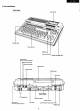
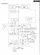
4-2. Custom
LSI
The custom
LSI
is a 100-pin single
chip
LSI
on which the
MZ-800
memory
controller (I/O controller) and
CRT
controller, etc. are contained.
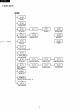
4-2-1. Memory controller
Used
for
the control
of
the
memory
bank. Addressing
of
DRAM, ROM, and VRAM is conducted by selection I/O
address,
$EO
- $E6, using OUT
or
IN
command.
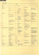
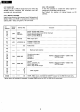
I/O
Signal
Device (I/O)
address name
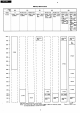
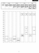
4-2-2. 1/0 controller
In this I/O controller is created the select signal
for
assignment
of
MZ-800 internal device.
See
Table-2
for
relation
of
internal device vs
I/O
address.
Function
FF
Port
B,
printer data
output
FE
CPR
Z80A Port A, printer control and
timer
interrupt
FD
PlO (I/O)
Port B control (Mode
0)
FC
Port A control (Mode
3)
F2
PSG
PSG
(0)
PSG
output
port
F1
JOY
JOYSTICK
(I)
Joystick-2
input
port
FO
Joystick-1
input
port
FO
--
(0)
Pallet
write
E6
1
--
--
(110)
Memory
bank control
EO
D7
Control
port
output
D6
C53
8253 (I/O)
Counter-2
(NOTE):
Mapped
to
E007
- E004 in the
D5
Counter-1 MZ-700 mode.
D4
Counter-O
D3
Control
D2
KEY
8255
(110)
Port
C,
cassette, etc.
(NOTE):
Mapped
to
E003
-
EOOO
in the
D1
Port
B,
key
input
MZ-700 mode.
DO
Port A, key strobe
output
CF
0
CE
I/O
CRTC
register
CD
--
--
0
CC
0
$E008
--
--
I/O
TEMP, HBLK
input;
and 8253
GO
ON/OFF
output
for
the MZ-700
mode
only.
* When above I/O address is accessed,
it
makes 10WR active
for
OUT
or
lORD
for
IN
command.
9