
Modem User Manual


LZT 123 1834 38
5.5 Regulated Power Supply Input (VCC)
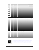
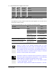
Pin Name Direction Function
1 VCC Input DC power
3 VCC Input DC power
5 VCC Input DC power
7 VCC Input DC power
9 VCC Input DC power
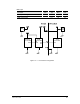
Power is supplied to the wireless modem VCC pins, from an external source.
User application circuitry should connect all VCC pins together in to carry the current
drawn by the wireless modem.
The electrical characteristics for VCC are shown in the following table.
Parameter Mode Limit
Nominal 3.6 V
Min 3.2 V
Max 4.5 V
Absolute maximum
voltage range
-0.3V to 6.5V
VCC Supply voltage
Maximum supply ripple
<100mV @<200kHz
<20mV @>200kHz
Maximum allowable voltage drop Transmission burst 200mV
2050 mA peak
Maximum current consumed
Full power (2W) transmit
(single uplink slot)
330mA average
Stresses in excess of the absolute maximum limits can cause
permanent damage to the device. These are absolute stress ratings
only. Functional operation of the device is not implied at these or any
other conditions in excess of those given in the operational sections of
the data sheet. Exposure to absolute maximum ratings for extended
periods can adversely affect device reliability.
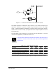
The wireless modem has insufficient internal capacitance to supply the
large current peaks during GSM burst transmission - use the following
general guidelines in designing the application power supply.
• Fit a low ESR electrolytic capacitor close to the wireless modem
(>1,000 µF, with an ESR < 100 m)
• Ensure power supply to wireless modem line resistance is < 200 m
TIP
!
WARNING