SERVICE MANUAL MODEL ................. KP-41S5 KP-41S5B KP-41S5G COMMANDER ............ DEST. ........................... CHASSIS NO. .......................... RM-862 AEP SCC-N60C-A RM-862 French SCC-N63B-A RM-862 Greek SCC-N60D-A MICROFILM ∗ Please file according to model size. ....... 41 MODEL ................. KP-41S5K KP-41S5R KP-41S5U RE-2 CHASSIS COMMANDER ............ DEST. ........................... CHASSIS NO. ..........................
KP-41S5/41S5B/41S5G/ 41S5K/41S5R/41S5U RM-862 SPECIFICATIONS Television system Colour system B/G/H,D/K,I,L PAL/SECAM NTSC 3.58/NTSC4.43(VIDEO IN) Channel coverage See " Receivable channels and channel displays " on this page. Projected picture size 41 inches Approx.
KP-41S5/41S5B/41S5G/ 41S5K/41S5R/41S5U RM-862 TABLE OF CONTENTS Section Title Page Section 1. GENERAL 2. DISASSEMBLY 6. DIAGRAMS 6-1. Block Diagram (1) ..................................................................................... 35 Block Diagram (2) ..................................................................................... 39 6-2. Frame Schematic Diagram ........................................................................ 43 6-3. Circuit Boards Location .......................
SECTION 1 GENERAL The operating instructions mentioned here partial abstracts from the Operating Instructions Manual.
–5–
–6–
–7–
–8–
–9–
– 10 –
– 11 –
– 12 –
– 13 –
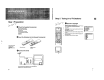
Troubleshooting Here are some simple solutions to some problems which may affect the picture and sound. Problem Solution No picture (screen is dark), no sound • Plug in the TV in. • Press U on the TV (if u indicator is on, press ; or a programme number on the Remote Commander). • Check the aerial connection. • Check if the selected video source is on. • Turn the TV off for 3 or 4 seconds then turn it on again using U .
KP-41S5/41S5B/41S5G/ 41S5K/41S5R/41S5U SECTION 2 RM-862 DISASSEMBLY 2-1. REAR BOARD REMOVAL 2-3. SERVICE POSITION 2 Rear board Main bracket section 3 Purse lock 1 Thirteen screws (Hexagon head) 2-2. MAIN BRACKET SECTION REMOVAL 2-4.
KP-41S5/41S5B/41S5G/ 41S5K/41S5R/41S5U RM-862 2-5. AE BOARD AND UE BOARD REMOVAL 6 Bracket (A) 9 AE board 7 Two claws 8 UE board 4 Terminal board (Euro) 5 claw 1 Five screws (+ BVTP 4X16) 3 Two screws (+ BVTP 3X12) 2 Screw (+ BVTP 4X16) 2-6.
KP-41S5/41S5B/41S5G/ 41S5K/41S5R/41S5U RM-862 2-7. BEZNET SECTION REMOVAL 8 Screen holder (H) 2 Seven screws (+ BVTP 4X16) 5 Four screws (+ BVTP 4X12) 7 Eight screws (+ BVTP 4X12) !∞ Mirror cover !¡ Screen holder (V) !™ Duffusion plate (F) !£ Duffusion plate (L) !¢ Contrast screen 6 Four screws (+ BVTP 4X12) 4 Beznet assembly 9 Screen holder (V) 1 Screws (+ BVTP 4X16) 3 Four screws (+ BVTP 4X16) 0 Screen holder (H) 2-8. HIGH-VOLTAGE CABLE INSTALLATION AND REMOVAL 2-9.
KP-41S5/41S5B/41S5G/ 41S5K/41S5R/41S5U RM-862 2-10. CHASSIS BLOCK REMOVAL (1) H1, H2 BOARDS AND AND RESISTOR REMOVAL (3) CHASSIS BLOCK REMOVAL 4 Four connectors 6 Resister (High voltage) 5 Screw (+ BVTP 4X6) 3 Three connectors 2 Control panel assembly 1 Two screws (+ BVTP 4X16) 2 Pull out the chassis block. 1 Six screws (Hexagon head) (2) MAIN BRACKET REMOVAL Pull out the chassis block by gripping the handles as shown in the diagram.
KP-41S5/41S5B/41S5G/ 41S5K/41S5R/41S5U SECTION 3 RM-862 SET-UP ADJUSTMENTS 3-1. SCREEN VOLTAGE ADJUSTMENT (ROUGH ALIGNMENT) 1. Receive the Monoscope signal. 2. Set 50% BRIGHTNESS and minimum PICTURE. 3. Turn the red VR on the FOCUS block all the way to the left and then gradually turn it to the right until the point where you can see the retrace line. 4. Next gradually turn it to the left to the position where the retrace line disappears. 3-3. SCREEN (G2) ADJUSTMENT 1. 2. 3. 4. Connect jig (A) to 200V.
KP-41S5/41S5B/41S5G/ 41S5K/41S5R/41S5U RM-862 3-5. DEFLECTION YOKE TILT ADJUSTMENT 3-7. 4-POLE MAGNET ADJUSTMENT 1. Set to receive the Monoscope signal. 2. Set in service mode. 3. Place the caps on the red and blue lens so that only the green color. 4. Loosen the deflection yoke setscrew and align the tilt of the Deflection Yoke so that the bars at the center of the monoscope pattern are horizontal. 5. After aligning the deflection yoke, fasten it securely to the funnel-shaped portion (neck) of the CRT.
KP-41S5/41S5B/41S5G/ 41S5K/41S5R/41S5U SECTION 4 RM-862 SAFETY RELATED ADJUSTMENT When replacing the following components marked with] on the schematic diagram, always check hold-down voltage and if necessary re-adjust. E BOARD – CONDUCTOR SIDE – CN810 CN505 Part Replaced ([) R1 Part Replaced (]) E Board G Board C515, L506, R517, C516, Q502, T502, C554, D504, R1, R514, T504 (FBT) D507, R516, Fig. 4-3 IC6008 CN505 4-1. HV HOLD-DOWN ADJUSTMENT R1 1. Remove CN810.
KP-41S5/41S5B/41S5G/ 41S5K/41S5R/41S5U SECTION 5 RM-862 CIRCUIT ADJUSTMENTS 5-1. ELECTRICAL ADJUSTMENTS PICTURE ADJUSTMENT Service adjustment to this model can performed with the supplied remote commander RM-862. AFC mode REF position SCP BGR SCP BGF Trap Fo Sub contrast Sub colour Sub brightness Green drive Blue drive Green cutoff Blue cutoff Gamma Pre / overshoot Y delay HOW TO ENTER INTO SERVICE MODE 1. Turn on the main power switch of the set and enter into standby mode. 2.
KP-41S5/41S5B/41S5G/ 41S5K/41S5R/41S5U RM-862 IC STATUS (CXA2076 / CXA2040) CXA2076 H lock 1 IKR 1 VNG 0 X•RAY 0 Colour system 3 CV1 Sync 0 CXA2040 Sync sep 1 S1 mode pin 01 S2 mode pin 01 TUNER Tuner status 01101011 CURRENT TV STATUS Text system Dolby Text language set Menu language set Destination Scart 16 : 9 RGB priority Ageing Size Colour trap sw Velocity mod AFT STATUS Lumisponder Mode MSP AGC ON / OFF Constant gain CDB FM prescale FMP Zwei mono-st WHI Zwei st-mono WLO Zwei mono-bi WMH Zwei bi-mono
KP-41S5/41S5B/41S5G/ 41S5K/41S5R/41S5U RM-862 5-2.
KP-41S5/41S5B/41S5G/ 41S5K/41S5R/41S5U RM-862 Adjustment Item number Item RH RV BH Data range Initial data 00 01 02 03 04 05 06 07 08 09 10 11 12 13 14 15 00 01 02 03 04 05 06 07 08 09 10 11 12 13 14 00 CENT SKEW BOW 4BOW SIZE LIN MSIZ MLIN KEY SSKW MPIN PIN SBOW MBOW 4PIN 4SBOW CENT SKEW BOW SIZE LIN MSIZ MKEY KEY SSKW MPIN PIN SBOW WAVE 4PIN MWAV BSEL –95~ +96 –95~ +96 –127 ~ +127 –127 ~ +127 –127 ~ +127 –127 ~ +127 –127 ~ +127 –127 ~ +127 –127 ~ +127 –127 ~ +127 –127 ~ +127 –127 ~ +127 –127 ~ +12
KP-41S5/41S5B/41S5G/ 41S5K/41S5R/41S5U RM-862 Adjustment Item number Item BV 00 01 02 03 04 05 06 07 08 09 10 11 12 13 14 CENT SKEW BOW SIZE LIN MSIZ MKEY KEY SSKW MPIN PIN SBOW WAVE 4PIN MWAV Data range Initial data –95~ +96 –95~ +96 –127 ~ +127 –127 ~ +127 –127 ~ +127 –127 ~ +127 –127 ~ +127 –127 ~ +127 –127 ~ +127 –127 ~ +127 –127 ~ +127 –127 ~ +127 –127 ~ +127 –127 ~ +127 –31 ~ +31 –10 0 0 0 0 0 –10 10 –10 0 10 32 –30 10 0 Data range Initial data Name / Description BLUE V CENTER BLUE V SKEW BL
KP-41S5/41S5B/41S5G/ 41S5K/41S5R/41S5U RM-862 5-3. REGISTRATION (CONVERGENCE) ADJUSTMENT METHOD 5-4. GEOMETRY Before adjust GEOMETRY, sure the data in convergence. • GH SIZE = 0 • GV SIZE = 0 • Adjust S correction PAL REGISTRATION ADJUSTMENT 1) Receive the PAL SPCB signal. 2) Select Service mode and enter adjustment items for Green signal. With the joystick: >. Items change ? / Data change In internal pattern it appears only RG or G only.
KP-41S5/41S5B/41S5G/ 41S5K/41S5R/41S5U RM-862 VERTICAL LINE ADJUSTMENT MENU n Convergence 7) Adjust LO CORN PIN Correct the screen bottom section line bow. 1. Carefully watching out for the GH CENT screen centre section, adjust GH CENT, GH BOW, GH SKEW. 2. GH 4th Bow adjustment. Correct the corner distortion which could not be adjusted with GH BOW. LO CORN PIN Watch out only for the GH CENT center point.
KP-41S5/41S5B/41S5G/ 41S5K/41S5R/41S5U RM-862 HORIZONTAL LINE ADJUSTMENT HORIZONTAL SIZE ADJUSTMENT 1. Finely adjust the centre position of the vertical line at the centre of the screen with GV CENT. 2. Using GV SKEW and GV BOW, correct the tilt and bow of the horizontal line at the centre of the screen. 1. Adjust with GH MSIZE, so that the sizes of both edges and centre are equal. 2. Adjust with GH SIZE, so that the horizontal sizes of both edges and centre are equal. 3.
KP-41S5/41S5B/41S5G/ 41S5K/41S5R/41S5U RM-862 GREEN VERTICAL SIZE ADJUSTMENT GREEN HORIZONTAL QUATERNARY ADJUSTMENT 1. Adjust GV MSIZE so that the sizes at the top and bottom and centre are equal. 2. Set the vertical size to correct specification. 3. While tracking adjust GV MSIZE and GV SIZE so that the space intervals for the vertical line of the screen are equal, also the vertical size should be within space. 4. Adjust again if GV L IN has been altered after completing the above adjustments. 1.
KP-41S5/41S5B/41S5G/ 41S5K/41S5R/41S5U RM-862 GREEN HORIZONTAL SYMMETRICAL PIN DISTORTION ADJUSTMENT GREEN VERTICAL 4TH ORDER DISTORTION ADJUSTMENT 1. Adjust GH MPIN to correct pin distorton at both edges of the centre section. 2. Use GH PIN to correct pin distortion at both edges of the screen. 3. While tracking adjust GH MPIN and GH PIN so that the PIN of vertical lines on the entire screen have no bowing. 4.
KP-41S5/41S5B/41S5G/ 41S5K/41S5R/41S5U RM-862 GREEN VERTICAL ASYMMETRICAL PIN DISTORTION (2ND-ORDER DISTORTION) ADJUSTMENT GREEN AND BLUE ADJUSTMENT 1. Correct the asymmetrical pin distortion at the top and bottom of the screen with GV SBOW. 1. Adjust so that the blue and green lines are on top of each other. Note : Main registration correction should not be while adjusting Blue adjustment. BEWARE : Not to change Green & Red Sub Items. It’ s easily done by mistake.
KP-41S5/41S5B/41S5G/ 41S5K/41S5R/41S5U RM-862 5-6. WHITE BALANCE ADJUSTMENT 1. Receive the monoscope signal and adjust the picture quality with the menu. 2. Adjust service mode S-BRIGHT so that the signal 10 IRE section barely glows. 3. Receive the all-white pattern signal. 4. Adjust the white balance with service mode G-CUTOFF and B-CUTOFF. 5. Adjust service mode S-BRIGHT so that the signal 100 IRE section barely glows. 6. Adjust the white balance with service mode G-DRIVE and B-DRIVE. 7.
KP-41S5/41S5B/41S5G/ 41S5K/41S5R/41S5U RM-862 MEMO – 34 –
KP-41S5/41S5B/41S5G/ 41S5K/41S5R/41S5U SECTION 6 RM-862 DIAGRAM 6-1.
KP-41S5/41S5B/41S5G/ 41S5K/41S5R/41S5U RM-862 CR(R OUT) CN1405 DY V.IN NC V.OUT NC VM.OUT NC VM.RET 1 2 3 4 ZB I (DY) TO E BOARD CN503 CN703 O TO AE BOARD CN301 4 3 2 1 CN1464 V901 PICTURE TUBE IK DET Q701 HB.RET VB.RET VB.IN HB.IN CN1462 HB.IN VB.IN VB.RET HB.RET 1 2 3 4 5 1 2 3 4 IN IN RET RET CN1431 VM CONT Q1433-1436 R 1 2 3 4 5 6 7 CN706 R G B 9V E IK E R/S NC H(+) H(-) NC NC 200V NC E H(+) H(-) 200V 1 1 2 3 ZG(DY/VM) V.DEF 1 V.MID 2 V.
6-2. FRAME SCHEMATIC DIAGRAM AUDIO L OUT AUDIO L OUT AUDIO R IN AUDIO R IN AUDIO R OUT AUDIO R OUT GND GND GND GND + GND CVBS/Y IN GND CN2701 CVBS OUT 7P GND RED-L :S-MICRO C IN MODE UE(AV3) BOX 1 2 3 4 5 6 7 + 1 2 3 4 5 6 7 BOX RED DRIVE GRN DRIVE BLUE DRIVE 9V GND CUT OFF GND CN301 7P RED :S-MICRO AE PHOTO SENSOR 1 2 3 R-H(+) NC NC R-H(-) V.DEF NC V.
4 AC(N)OUT NC NC NC AC(L)OUT TO H1 BOARD CN3003 5 4 3 2 1 CN6006 4B2P :VH A 5 AC(N)IN NC NC AC(L)IN 3 2 4 3 2 1 1 6 7 8 10 9 11 12 13 15 14 16 TO H1 BOARD CN3004 G(POWER 1 DTC 7 8 VS 5 DPC HIN SD NC C6033 0.001 D6042 UF4005PKG23 PROTECT D6044 UF4005PKG23 PROTECT LIN VE VSS COM 3 C2 12 VCC 13 RT 12 C D6043 MTZJ-20C PROTECT G BOARD IC VOLTAGE LIST REF. NO. VOL.
KP-41S5/41S5B/41S5G/ 41S5K/41S5R/41S5U G RM-862 [POWER SUPPLY] – G Board – 1 2 3 4 5 6 G BOARD DIODE D6002 D6003 D6004 D6005 D6007 D6008 D6012 D6013 D6014 D6017 D6018 D6025 D6032 D6033 D6035 D6036 D6037 D6038 D6042 D6043 D6044 D6045 D6046 D6047 A B C C-5 H-2 C-4 H-3 E-2 E-3 A-3 E-2 H-4 E-2 H-4 C-3 H-3 H-3 D-4 D-4 C-4 C-6 H-6 H-5 H-6 H-5 H-5 H-6 * – – – – – – – – – – – – – – – – – – – – – – – – D6048 D6049 D6050 D6051 B-4 C-4 C-3 E-2 – – – – TRANSISTOR * Q6001 Q6002 Q6003 Q6005 Q6009 Q60
KP-41S5/41S5B/41S5G/ 41S5K/41S5R/41S5U RM-862 AE(1/2) [ ] VIDEO SW, AUDIO SW, AUDIO PROCESSER, TUNER, DIGITAL COMB FILTER AE(2/2) [CHROMA DECODER, TEXT/OSD] – AE Board – AE BOARD DIODE D2 D10 D11 D12 D16 D101 D102 D201 D202 D203 D204 D205 D206 D207 D208 D209 D210 D211 D212 D213 D214 D215 D216 D217 D218 D220 D221 D222 D223 D224 D225 D226 D227 D228 D231 D251 D303 D304 D320 D370 D1010 B-5 B-6 C-6 B-6 B-6 G-6 D-5 H-9 H-3 H-9 F-2 F-2 G-8 G-8 H-9 H-8 H-9 H-8 F-2 F-2 G-7 G-7 H-4 H-4 H-4 H-4 H-4 H-9 H-2 H-2
6 7 8 10 9 11 12 13 15 14 16 17 18 19 20 22 21 • AE(1/2) BOARD WAVEFORMS A B C D E F G H GND +5V AM QSS VIDEO NC TU101 TVF01-FR 5 +33V CN2 5P WHT 1 TP2 # B R280 1k :CHIP CPU R101 3.3k :CHIP R102 100 :CHIP DIS D220 1SS355 Q18 DTA144EKA INV C FL101 FZ103N AGC D216 UDZ-5.6B Q214 DTC144EKA INV R104 10k :CHIP D101 MA8330 TP1 # D221 1SS355 R103 100 :CHIP VIDEO C103 22 D217 UDZ-5.6B +9V 5V Q110 Q111 2SC2412K 2SA1037AK V-BUFF V-BUFF L111 0 :CHIP C112 0.
1 • AE(2/2) BOARD WAVEFORMS 8 10 9 11 12 15 14 16 17 18 19 20 D5 D0 D6 A0 D7 A1 A2 A10 A3 A4 A11 A5 A9 A6 A8 A7 A13 A12 A14 A15 A 1.6Vp-p(H) 0.4Vp-p(H) 0.4Vp-p(H) 1.0Vp-p(H) 0.6Vp-p(H) 1.6Vp-p(H) 2.2Vp-p(H) 3.9Vp-p(H) 3.9Vp-p(H) 3.9Vp-p(H) 29 28 27 26 25 24 23 22 21 2 RST IC2 •All voltage are in V. * :Can not mesured. •Pin numbers which are not described are not used. – 61 – Q1002 2SA1037AK BUFF R42 6.8k :CHIP R44 6.8k :CHIP B-Y TRAP B-Y Q300 DTC144EKA SW C302 0.
KP-41S5/41S5B/41S5G/ 41S5K/41S5R/41S5U RM-862 4 5 6 7 8 10 9 11 12 CN3202 11P RED-L :S-MICRO FUNCTION KEY) H1( RMC, TO D BOARD CN1802 CN3004 5B3PS WHT-L :VH 15 14 13 FR S3 OUT GND FR R OUT GND FR L OUT GND FR V OUT GND FR C OUT GND FR Y OUT A 3 2 11 10 9 8 7 6 5 4 3 2 1 1 TO G BOARD CN6007 R3002 10k :RN-CP INPUT SELECT VOL- R3006 4.7k :RN-CP 1 2 3 4 5 R3007 2.
KP-41S5/41S5B/41S5G/ 41S5K/41S5R/41S5U E RM-862 [H/V-DEF, HV] – E Board – 1 2 3 4 5 6 7 8 9 10 11 E BOARD A DIODE D501 D502 D503 D504 D507 D508 D509 D510 D511 D512 D513 D514 D515 D517 D519 D520 D521 D522 D523 D524 D527 D701 D702 D820 D829 D835 D840 D842 D845 D846 D-5 D-5 A-9 D-5 C-5 E-8 E-9 H-6 C-8 A-9 F-10 H-11 F-11 C-10 H-3 F-11 E-9 E-3 F-7 D-6 D-6 C-1 D-2 D-2 B-2 E-5 A-4 A-4 B-4 B-4 B C D TRANSISTOR Q501 Q502 Q503 Q504 Q505 Q506 Q507 Q801 Q802 Q803 Q804 Q805 Q806 Q807 Q808 Q809 Q81
E BOARD : IC804,806,808 PM0002B E BOARD : IC801,802 PA0053B • E BOARD WAVEFORMS 4.8Vp-p (H) 2.6Vp-p (H) 8 2.5Vp-p (H) 5 6 7 8 10 9 21 4.5Vp-p (H) 12 12.7Vp-p (H) 15 14 13 11.4Vp-p (H) 16 17 18 19 20 22 21 SUB. GND H2 H2 -5V R999 4.7k C880 47 25V 2 H2 1 BH A 11 1.4Vp-p (V) 20 1090Vp-p (H) GV 4 14 1.3Vp-p (V) 19 BV 3 2 11.2Vp-p (H) 2.6Vp-p (V) 13 1.3Vp-p (V) 18 89.0Vp-p (H) 4.7Vp-p (V) 12 1.6Vp-p (V) 17 7 2.5Vp-p (H) 11 2.4Vp-p (V) 16 6 2.
• D BOARD WAVEFORMS ? – 73 – board / AUDIO R R1653 1k :CHIP AUDIO L R1654 1k :CHIP Q1616 D1616 2SC2412K DET 1SS133T D1614 1SS133T R1655 10k :CHIP 7 8 C1809 100 25V SIRCS C1631 2200 R1646 0.1 1/2W :RF R1656 0 :CHIP -5V STBY5V +B C1802 0.01 B:CHIP 12V O C1805 0.01 B:CHIP I C1803 470 16V IC1801 LM2940CT-5.0 STBY 5V REG C1804 10 7V C1807 10 IC1802 PQ09RF2 9V REG -5V +B 135V +15V 5V G C1811 100 25V C1810 0.01 B:CHIP C1516 0.
D [ KP-41S5/41S5B/41S5G/ 41S5K/41S5R/41S5U ] AUDIO AMP, HP AMP, V OUT, PJ ENGINE RM-862 – D Board – 1 2 3 4 5 6 7 8 9 10 11 12 13 14 15 16 17 D BOARD DIODE D1501 D1502 D1503 D1504 D1505 D1601 D1603 D1604 D1606 D1611 D1612 D1613 D1614 D1615 D1616 D1618 D1619 D1620 D1621 D1622 D1703 D1704 D1705 D1706 D1707 D1708 D1709 D1710 D1711 D1712 D1801 D1802 D1803 D1804 D1805 D1806 A B C D E G-2,G-16 G-3,G-15 H-2,H-16 H-3,H15 H-15 F-6,F-12 F-6,F-12 F-6,F-12 F-6,F-12 D-7,D-11 H-9 D-7,D-11 G-
KP-41S5/41S5B/41S5G/ 41S5K/41S5R/41S5U RM-862 1 3 2 4 5 7 8 10 9 11 12 CN1434 4P :VH T0 E BOARD CN503 TO E BOARD CN504 DY(H) H+ H(MID) H- 1 2 3 4 H.IN V.IN CN1404 4P RED :S-MICRO SUB DY DY(V) V.RET H.RET V.DEF V(MID) V.RET R1415 120 3W R-H(+) NC NC R-H(-) R1418 120 3W DY(H) R1401 560 HR.IN VR.IN VR.RET HR.RET 1 2 3 4 H.IN V.IN DY(V) R1435 120 3W G-H(+) NC NC G-H(-) CN1433 4P WHT :S-MICRO SUB DY TO E BOARD CN801 1 2 3 4 R1402 560 H+ H(MID) H- V.RET H.RET V.DEF V(MID) V.
KP-41S5/41S5B/41S5G/ 41S5K/41S5R/41S5U RM-862 1 3 2 4 G1 G2 4 10 5 6 7 8 10 9 11 G4 1,2 12 G1 G2 4 10 13 15 14 CR G4 1,2 [R OUT] – CR Board – A V901 PICTURE TUBE 07MXC(R) 6 7 H G3 K 8 G5 HV.BLOCK H V902 PICTURE TUBE 07MXC(G) 6 7 G3 K 8 G5 HV.BLOCK CR BOARD TRANSISTOR VOLTAGE LIST B REF. TO FOCUS BLOCK Q701 CR (R OUT) SG703 CN705 FGND 1 G1 C GND 12 G2 C705 0.
KP-41S5/41S5B/41S5G/ 41S5K/41S5R/41S5U RM-862 1 3 2 4 G1 G2 4 10 5 V903 PICTURE TUBE 07MXC(B) 6 7 G3 K 8 7 8 10 9 11 12 13 G4 1,2 A H 6 G5 CN2703 21P SCART UE(AV-INPUT/OUTPUT) CN2701 7P RED-L :S-MICRO HV.BLOCK C2705 220 16V R2706 91 :CHIP CVBS IN D2701 UDZ-9.1B CVBS OUT R2702 75 :CHIP B R2707 82 :CHIP C IN TO FOCUS BLOCK CB (B OUT) R2703 220 :CHIP 1 GND 12 4 11 NC 10 CN763 1P WHT :MINI G2 6 H(+) H(-) B C763 0.
KP-41S5/41S5B/41S5G/ 41S5K/41S5R/41S5U RM-862 2SK2251-01-F119 ERC06-15S ERD29-08J S2LA20F BAS216 ANODE CATHODE DTZ33B DTZ6.8B DTZ9.1 RD5.6S-B UDZ-TE-17-6.8B 1SS355TE-17 MTZJ-13 MTZJ-30B MTZJ-7.5B RD13ES-B2 RD20ES-B2 RD3.6ES-B1 RD39ES-B2 RD4.7ESB2 RD4.7ES-TIB RD5.1ES-B1 RD5.1ES-B2 RD5.6ES-B2 RD7.5ES-B2 1SS119-25 1SS133T-77 D10SC6M-4012 SLA-580LT3F D2S4M D4SBS4-F D6SB6OL RBA-406B U05G MA3030-H(TX) IRFI744G-LF EL1Z GP08D MTZ-T-77-9.
KP-41S5/41S5B/41S5G/ 41S5K/41S5R/41S5U SECTION 7 RM-862 The componants identified by are critishading and mark cal for safety. Replace only with part number specified. EXPLODED VIEWS NOTE: • The construction parts of an assembled part are indicated with a collation number in the remark column. • Items with no part number and no description are not stocked because they are seldom required for routine service. • Items marked " * " are not stocked since they are seldom required for routine service.
KP-41S5/41S5B/41S5G/ 41S5K/41S5R/41S5U RM-862 7-2. The componants identified by shading and mark are critical for safety. Replace only with part number specified. CABINET AND PANEL BLOCK 4 : +BVTP 3X12 7-685-648-79 ® : +BVTP 4X16 7-685-663-71 r : +BVTP 4X16 7-685-663-79 ® ® ® r 64 ® 63 54 4 r 69 62 r 70 ® 57 54 4 54 r 52 58 4 53 55 70 4 56 60 r 65 4 61 54 4 59 r ® 54 4 71 66 r ® 67 51 4 REF.NO. PART NO. DESCRIPTION 68 REMARK REF.NO. PART NO.
KP-41S5/41S5B/41S5G/ 41S5K/41S5R/41S5U RM-862 7-3. CHASSIS AND PICTURE TUBE 4 : +BVTP 3X12 7-685-648-79 ® : +BVTP 4X16 7-685-663-71 r : +BVTP 4X16 7-685-663-79 The componants identified by shading and mark are critical for safety. Replace only with part number specified.
The componants identified by shading and mark are critical for safety. Replace only with part number specified. NOTE: REF.NO. PART NO. SECTION 8 RM-862 AE ELECTRICAL PARTS LIST DESCRIPTION The componants identified by shading and mark are critical for safety. Replace only with part number specified. KP-41S5/41S5B/41S5G/ 41S5K/41S5R/41S5U REMARK REF.NO. PART NO.
KP-41S5/41S5B/41S5G/ 41S5K/41S5R/41S5U The componants identified by are critishading and mark cal for safety. Replace only with part number specified. RM-862 AE REF.NO. PART NO. DESCRIPTION REMARK C213 C214 1-163-133-00 CERAMIC CHIP 470pF 1-164-346-11 CERAMIC CHIP 1µF 5% 50V 16V C215 C216 C217 C218 C219 1-163-133-00 1-104-664-11 1-164-232-11 1-104-664-11 1-164-232-11 CERAMIC CHIP 470pF ELECT 47µF CERAMIC CHIP 0.01µF ELECT 47µF CERAMIC CHIP 0.
KP-41S5/41S5B/41S5G/ 41S5K/41S5R/41S5U The componants identified by shading and mark are critical for safety. Replace only with part number specified. REF.NO. PART NO. RM-862 AE DESCRIPTION REMARK C376 C377 C380 C1001 1-163-251-11 1-126-964-11 1-163-038-00 1-163-235-11 CERAMIC CHIP 100pF ELECT 10µF CERAMIC CHIP 0.1µF CERAMIC CHIP 22pF 5% 50V 20% 50V 25V 5% 50V C1002 C1010 C1013 C1014 C1015 1-163-235-11 1-163-038-00 1-126-965-11 1-163-038-00 1-164-489-11 CERAMIC CHIP 22pF CERAMIC CHIP 0.
KP-41S5/41S5B/41S5G/ 41S5K/41S5R/41S5U The componants identified by are critishading and mark cal for safety. Replace only with part number specified. RM-862 AE REF.NO. PART NO.
KP-41S5/41S5B/41S5G/ 41S5K/41S5R/41S5U The componants identified by shading and mark are critical for safety. Replace only with part number specified. REF.NO. PART NO. RM-862 AE DESCRIPTION REMARK R47 R48 R49 R50 1-216-057-00 1-217-671-11 1-216-025-00 1-216-065-00 RES,CHIP RES,CHIP RES,CHIP RES,CHIP 2.2K 1 100 4.7K 5% 5% 5% 5% 1/10W 1/10W 1/10W 1/10W R51 R52 R53 R54 R58 1-216-059-00 1-216-065-00 1-216-059-00 1-216-025-00 1-216-063-91 RES,CHIP RES,CHIP RES,CHIP RES,CHIP RES,CHIP 2.7K 4.7K 2.
KP-41S5/41S5B/41S5G/ 41S5K/41S5R/41S5U The componants identified by are critishading and mark cal for safety. Replace only with part number specified. RM-862 AE REF.NO. PART NO. DESCRIPTION REMARK R189 R190 R191 R192 R193 1-216-043-91 1-216-067-00 1-216-057-00 1-216-049-00 1-216-049-00 RES,CHIP RES,CHIP RES,CHIP RES,CHIP RES,CHIP 560 5.6K 2.
KP-41S5/41S5B/41S5G/ 41S5K/41S5R/41S5U The componants identified by shading and mark are critical for safety. Replace only with part number specified. REF.NO. PART NO. RM-862 AE G DESCRIPTION REMARK R331 R332 1-216-059-00 RES,CHIP 1-216-049-00 RES,CHIP 2.7K 1K 5% 5% R333 R334 R335 R336 R337 1-216-067-00 1-216-041-00 1-216-675-91 1-216-109-00 1-216-025-00 RES,CHIP RES,CHIP METAL CHIP RES,CHIP RES,CHIP 5.6K 470 10K 330K 100 5% 1/10W 5% 1/10W 0.
KP-41S5/41S5B/41S5G/ 41S5K/41S5R/41S5U The componants identified by are critishading and mark cal for safety. Replace only with part number specified. RM-862 G REF.NO. PART NO. DESCRIPTION REMARK REF.NO. PART NO.
KP-41S5/41S5B/41S5G/ 41S5K/41S5R/41S5U The componants identified by shading and mark are critical for safety. Replace only with part number specified. REF.NO. PART NO. R6010 R6013 R6014 R6018 R6019 1-215-479-00 1-202-968-11 1-216-089-00 1-216-089-00 1-216-089-00 RM-862 G CR DESCRIPTION REMARK REF.NO. PART NO. METAL CEMENTED RES,CHIP RES,CHIP RES,CHIP 270K 1.
KP-41S5/41S5B/41S5G/ 41S5K/41S5R/41S5U The componants identified by are critishading and mark cal for safety. Replace only with part number specified. RM-862 CR CG CB REF.NO. PART NO. DESCRIPTION REMARK R715 1-260-133-11 CARBON 680K 5% 1/2W R716 R717 R718 R719 R720 1-247-815-91 1-249-435-11 1-249-437-11 1-219-743-11 1-249-425-11 CARBON CARBON CARBON CARBON CARBON 220 33K 47K 100 4.
KP-41S5/41S5B/41S5G/ 41S5K/41S5R/41S5U The componants identified by shading and mark are critical for safety. Replace only with part number specified. REF.NO. PART NO. RM-862 CB D DESCRIPTION REMARK REF.NO. PART NO. DESCRIPTION REMARK C1501 C1503 C1504 C1506 C1507 1-163-005-11 CERAMIC CHIP 470pF 1-137-399-11 FILM 0.1µF 1-164-690-91 CERAMIC CHIP 0.
KP-41S5/41S5B/41S5G/ 41S5K/41S5R/41S5U The componants identified by are critishading and mark cal for safety. Replace only with part number specified. RM-862 D REF.NO. PART NO.
KP-41S5/41S5B/41S5G/ 41S5K/41S5R/41S5U The componants identified by shading and mark are critical for safety. Replace only with part number specified. REF.NO. PART NO. RM-862 D DESCRIPTION REMARK D1804 8-719-923-60 DIODE MTZJ-T-77-9.1A D1805 D1806 8-719-923-60 DIODE MTZJ-T-77-9.1A 8-719-923-60 DIODE MTZJ-T-77-9.1A REF.NO. PART NO.
KP-41S5/41S5B/41S5G/ 41S5K/41S5R/41S5U The componants identified by are critishading and mark cal for safety. Replace only with part number specified. RM-862 D REF.NO. PART NO.
KP-41S5/41S5B/41S5G/ 41S5K/41S5R/41S5U The componants identified by shading and mark are critical for safety. Replace only with part number specified. REF.NO. PART NO.
KP-41S5/41S5B/41S5G/ 41S5K/41S5R/41S5U The componants identified by are critishading and mark cal for safety. Replace only with part number specified. RM-862 E REF.NO. PART NO. DESCRIPTION REMARK C513 1-126-965-11 ELECT C514 ! 1-162-116-91 CERAMIC 22µF 680pF 20% 50V 10% 2KV C515 ! 1-125-831-91 FILM C516 ! 1-117-648-11 FILM C518 1-130-495-00 FILM C519 1-106-359-00 MYLAR C520 1-162-116-00 CERAMIC 0.033µF 15000pF 0.1µF 0.0047µF 680pF 3% 3% 5% 10% 10% 630V 1.
KP-41S5/41S5B/41S5G/ 41S5K/41S5R/41S5U The componants identified by shading and mark are critical for safety. Replace only with part number specified. REF.NO. PART NO. RM-862 E DESCRIPTION C886 C887 C888 C889 1-102-973-00 1-102-973-00 1-102-973-00 1-104-665-11 CERAMIC CERAMIC CERAMIC ELECT C897 1-104-665-11 ELECT REMARK 100pF 100pF 100pF 100µF 5% 5% 5% 20% 50V 50V 50V 25V 100µF 20% 25V REF.NO. PART NO.
KP-41S5/41S5B/41S5G/ 41S5K/41S5R/41S5U RM-862 • The components identified by in this manual have been carefully factory-selected for each set in order to satisfy regulations regarding X-ray radiation. Should replacement be required, replace only with the value originally used. REF.NO. PART NO. DESCRIPTION REMARK REF.NO. PART NO. The componants identified by are critishading and mark cal for safety. Replace only with part number specified.
KP-41S5/41S5B/41S5G/ 41S5K/41S5R/41S5U The componants identified by shading and mark are critical for safety. Replace only with part number specified. REF.NO. PART NO. RM-862 E DESCRIPTION REMARK R805 R806 R807 R808 R809 1-247-807-31 1-249-429-11 1-247-807-31 1-249-429-11 1-249-425-11 CARBON CARBON CARBON CARBON CARBON 100 10K 100 10K 4.
KP-41S5/41S5B/41S5G/ 41S5K/41S5R/41S5U The componants identified by are critishading and mark cal for safety. Replace only with part number specified. RM-862 E H1 REF.NO. PART NO. DESCRIPTION REMARK R928 1-249-429-11 CARBON 10K 5% 1/4W R929 R930 R931 R933 R934 1-214-800-11 1-214-800-11 1-215-445-00 1-215-445-00 1-249-422-11 METAL METAL METAL METAL CARBON 2.2 2.2 10K 10K 2.
KP-41S5/41S5B/41S5G/ 41S5K/41S5R/41S5U The componants identified by shading and mark are critical for safety. Replace only with part number specified. REF.NO. PART NO. RM-862 H1 UE H2 DESCRIPTION R3002 R3006 R3007 R3009 1-216-675-91 1-216-667-11 1-216-661-11 1-216-041-00 METAL CHIP METAL CHIP METAL CHIP RES,CHIP R3010 1-216-045-00 RES,CHIP REMARK 10K 4.7K 2.7K 470 0.50%1/10W 0.50%1/10W 0.50%1/10W 5% 1/10W 680 5% REF.NO. PART NO.
KP-41S5/41S5B/41S5G/ 41S5K/41S5R/41S5U The componants identified by are critishading and mark cal for safety. Replace only with part number specified. RM-862 ZR ZG REF.NO. PART NO. DESCRIPTION REMARK REF.NO. PART NO.
KP-41S5/41S5B/41S5G/ 41S5K/41S5R/41S5U The componants identified by shading and mark are critical for safety. Replace only with part number specified. REF.NO. PART NO. DESCRIPTION RM-862 REMARK REF.NO. PART NO.
KP-41S5/41S5B/41S5G/ 41S5K/41S5R/41S5U The componants identified by are critishading and mark cal for safety. Replace only with part number specified. RM-862 REF.NO. PART NO. DESCRIPTION REMARK REF.NO. PART NO. Sony Corporation 9-965-403-01 HDC Projector Division Company – 116 – DESCRIPTION REMARK English 99HA71652-1 Printed in UK 1999.