
SparkFun BabyBuck Regulator Breakout - 3.3V (AP63203) - Datasheet
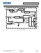
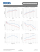
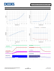
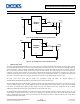
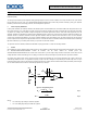
Table Of Contents

AP63200/AP63201/AP63203/AP63205
Application Information (continued)
In order to provide a small output ripple in light load conditions, the AP63201 offers a fixed 500kHz switching frequency with FSS and Pulse Width
Modulation (PWM).
The hiccup mode minimizes power dissipation during prolonged output overcurrent or short conditions. The hiccup wait time is 512 cycles and the
hiccup restart time is 8192 cycles. The AP63200/AP63201/AP63203/AP63205 also features full protections including cycle-by-cycle high-side
MOSFET peak current limit, overvoltage protection, and overtemperature protection.
2 Pulse Frequency Modulation
In heavy load conditions, the AP63200, AP63203, and AP63205 operate at forced PWM mode. The internal COMP node voltage decreases as the
load current decreases. At a certain limit, if the load current is low enough, the COMP node voltage is clamped and is prevented from decreasing
any further. The voltage at which COMP is clamped corresponds to the 450mA peak inductor current. As the load current approaches zero, the
AP63200, AP63203, and AP63205 enter Pulse Frequency Modulation (PFM) to increase the converter power efficiency at light load conditions. The
AP63201 remains in continuous conduction mode at light load conditions. When the inductor current decreases to zero, zero-cross detection
circuitry on the low-side power MOSFET, Q2, forces it off until the beginning of the next switching cycle. The buck converter does not sink current
from the output when the output load is light and while the device is in PFM. Because the AP63200, AP63203, and AP63205 work in PFM during
light load conditions, they can achieve power efficiency of up to 88% at a 5mA load condition.
The quiescent current of AP63200, AP63203 and AP63205 is 22μA typical under a no-load, non-switching condition.
3 Enable
When disabled, the device shutdown supply current is only 1μA. When applying a voltage higher than the EN upper threshold (typical 1.18V, rising),
the AP63200/AP63201/AP63203/AP63205 enables all functions, and the device initiates the soft-start phase. The
AP63200/AP63201/AP63203/AP63205 has a built-in 4ms soft-start time to prevent output voltage overshoot and inrush current. When the EN
voltage falls below its lower threshold (typical 1.1V, falling), the internal SS voltage is discharged to ground and device operation is disabled.
An internal 1.5µA pull-up current source connected from the internal LDO-regulated VCC to the EN pin guarantees that a high on the EN pin
automatically enables the device. For applications requiring a higher VIN UVLO voltage than is provided by the default setup, there is a 4µA
hysteresis pull-up current source on the EN pin that configures the VIN UVLO voltage with an external resistive divider (R5 and R6) shown in Figure
22. The resistive divider resistor values are calculated by equations Eq.1 and Eq.2.
EN
20kΩ
+
-
ON
1.18V
I
1
1.5
µA
I
2
4µA
VIN
R5
R6
2
Figure 22. Programming UVLO
=
.
.
Eq. 1
=
.
. + .
Eq. 2
Where:
• V
ON
is the rising edge voltage to enable the regulator
• V
OFF
is the falling edge voltage to disable the regulator
AP63200/AP63201/AP63203/AP63205
Document number: DS41326 Rev. 2 - 2
10 of 18
www.diodes.com
January 2019
© Diodes Incorporated