
SparkFun BabyBuck Regulator Breakout - 3.3V (AP63203) - Datasheet
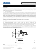

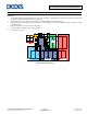
Table Of Contents

AP63200/AP63201/AP63203/AP63205
Application Information (continued)
Alternatively, a small ceramic capacitor can be added from EN to GND. This delays the output startup voltage, which is useful when sequencing
multiple power rails to minimize input inrush current. The amount of capacitance is calculated by equation Eq.3.
[] = .
[]
Eq. 3
Where:
• C
d
is the time delay capacitance in nF
• t
s
is the delay time in ms
The EN pin is a high voltage pin and can be directly connected to VIN to automatically start up the device as VIN increases.
4 Undervoltage Lockout
Undervoltage lockout is implemented to prevent the IC from insufficient input voltages. The AP63200/AP63201/AP63203/AP63205 device has a
UVLO comparator that monitors the input voltage and the internal bandgap reference. If the input voltage falls below 3.1V, the
AP63200/AP63201/AP63203/AP63205 is disabled. In this event, both the high-side and low-side power MOSFETs are turned off.
5 EMI Reduction with Frequency Spread Spectrum and Ringing-free Switching Node
In the some applications, the system must meet EMI standards. To improve EMI reduction, the AP63200/AP63201/AP63203/AP63205 adopts FSS
to spread the switching noise over a wider frequency band and therefore reduces conducted and radiated interference at a particular frequency.
In buck converters, the switching node’s (SW’s) ringing amplitude and cycles are critical, especially in relation to the high frequency radiation EMI
noise. The AP63200/AP63201/AP63203/AP63205 device implements a multi-level gate driver scheme to achieve a ringing-free switching node
without sacrificing neither the switching node’s rise and fall slew rates nor the converter’s power efficiency. The AP63203 and AP63205 also have
the feature to remove the resonance ringing of the SW pin when the inductor current is 0A and the device operates in PFM. The zoomed in
waveform for SW is shown in Figure 23.
Figure 23. AP63203/AP63205 SW Node Waveform
6 Overcurrent Protection
The AP63200/AP63201/AP63203/AP63205 has cycle-by-cycle peak current limit protection by sensing the current through the internal high-side
power MOSFET Q1. While Q1 is on, its conduction current is monitored by the internal sensing circuitry. Once the current through Q1 exceeds the
current peak limit, Q1 immediately turns off. If Q1 consistently hits the peak current limit for 2ms, the buck converter enters hiccup mode and shuts
down. After 16ms of off time, the buck converter restarts powering up. Hiccup mode reduces the power dissipation in the overcurrent condition.
7 Thermal Shutdown
If the junction temperature of the device reaches the thermal shutdown limit of +150°C, the AP63200/AP63201/AP63203/AP63205 shuts down both
their high-side and low-side power MOSFETs. When the junction temperature reduces to the required level (+130°C nominal), the device initiates a
normal power-up cycle with soft-start.
SW (5V/div)
IL (1A/div)
No SW Ringing
2µs/div
AP63200/AP63201/AP63203/AP63205
Document number: DS41326 Rev. 2 - 2
11 of 18
www.diodes.com
January 2019
© Diodes Incorporated