
SparkFun BabyBuck Regulator Breakout - 3.3V (AP63203) - Datasheet
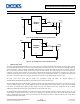
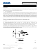

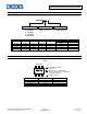
Table Of Contents

AP63200/AP63201/AP63203/AP63205
Application Information (continued)
8 Power Derating Characteristics
To prevent the regulator from exceeding the maximum junction temperature, some thermal analysis is required. The temperature rise is given by:
= (
)
Eq. 4
Where PD is the power dissipated by the regulator and θ
JA
is the thermal resistance from the junction of the die to the ambient temperature.
The junction temperature, T
J
, is given by:
=
+
Eq. 5
Where T
A
is the ambient temperature of the environment. For the TSOT26 package, the θ
JA
is 89°C/W. The actual junction temperature should not
exceed the absolute maximum junction temperature of +125°C when considering the thermal design. A typical derating curve versus ambient
temperature is shown in Figure 24.
Figure 24. Output Current Derating Curve vs. Temperature, VIN = 12V
9 Setting the Output Voltage
The AP63203 and AP63205 have fixed output voltages of 3.3V and 5V, respectively. The AP63200 and AP63201 have adjustable output
voltages starting from 0.8V using an external resistive divider. An optional in Figure 20, of 10pF to 220pF is used to improve the transient
response. Resistor R2 is selected based on a design tradeoff between efficiency and output voltage accuracy. There is less current consumption
in the feedback network for high values of R2. R1 can be determined by the following equation:
=
(
.
)
Eq. 6
AP63200/AP63201/AP63203/AP63205
Document number: DS41326 Rev. 2 - 2
12 of 18
www.diodes.com
January 2019
© Diodes Incorporated