
SparkFun BabyBuck Regulator Breakout - 3.3V (AP63203) - Datasheet
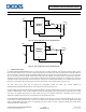

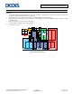
Table Of Contents

AP63200/AP63201/AP63203/AP63205
Layout
PCB Layout
1. The AP63200/AP63201/AP63203/AP63205 device works at 2A current load, so heat dissipation is a major concern in the layout of the PCB.
2oz copper for both the top and bottom layers is recommended.
2. Provide sufficient vias for the input and output capacitors’ GND side to dissipate heat to the bottom layer.
3. Make the bottom layer under the device as the GND layer for heat dissipation. The GND layer should be as large as possible to provide
better thermal effect.
4. Place the VIN capacitors as close to the device as possible.
5. Place the feedback components as close to FB as possible.
6. See Figure 25 for reference.
C1
C2
L1
C3
C4
R1
R2
VIN
VOUT
SW
1
2
3 4
5
6FB
EN
VIN GND
SW
BST
GND
Figure 25. Recommended Layout
AP63200/AP63201/AP63203/AP63205
Document number: DS41326 Rev. 2 - 2
15 of 18
www.diodes.com
January 2019
© Diodes Incorporated