
SparkFun BabyBuck Regulator Breakout - 3.3V (AP63203) - Datasheet
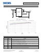
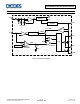
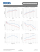
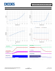
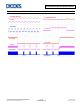
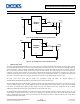
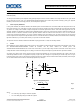
Table Of Contents

AP63200/AP63201/AP63203/AP63205
Typical Application Circuit
AP63205
L
4.7µH
C3
100nF
C2
2x22μF
C1
10μF
3
VIN
2
EN
5
SW
6
BST
1
FB
4
GND
OUTPUT
V
OUT
5V
INPUT
Figure 1. Typical Application Circuit
Figure 2. Efficiency vs. Output Current
Pin Descriptions
Pin Number Pin Name Function
1 FB
Feedback sensing terminal for the output voltage. Connect this pin to the resistive divider of the output.
See
Setting the Output Voltage
section for more details.
2 EN
Enable Input. EN is a digital input that turns the regulator on or off. Drive EN high to turn on the regulator and low
to turn it off. Attach to VIN or leave open for automatic startup. The EN has a precision threshold of 1.18V for
programing the UVLO. See Enable section for more details.
3 VIN
Power Input. VIN supplies the power to the IC, as well as the step-down converter switches. Drive VIN with a
3.8V to 32V power source. Bypass VIN to GND with a suitably large capacitor to eliminate noise due to the
switching of the IC. See Input Capacitor section for more details.
4
GND
Power Ground.
5 SW
Power Switching Output. SW is the switching node that supplies power to the output. Connect the output LC filter
from SW to the output load. Note that a capacitor is required from SW to BST to power the high-side switch.
6 BST
High-Side Gate Drive Boost Input. BST supplies the drive for the high-side N-Channel MOSFET. A 100nF
capacitor is recommended from SW to BST to power the high-side switch.
AP63200/AP63201/AP63203/AP63205
Document number: DS41326 Rev. 2 - 2
2 of 18
www.diodes.com
January 2019
© Diodes Incorporated