
SparkFun BabyBuck Regulator Breakout - 3.3V (AP63203) - Datasheet
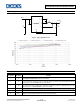
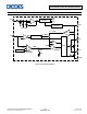
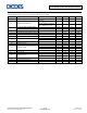
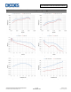
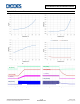
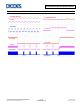
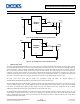
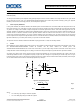
Table Of Contents

AP63200/AP63201/AP63203/AP63205
Application Information
AP
63200
AP63201
L
2.2μH
R
1
30.9kΩ
R2
62kΩ
C3
100nF
C2
2x22μF
C1
10μF
3
VIN
2
EN
5
SW
6
BST
1
FB
4
GND
OUTPUT
V
OUT
1.2V
INPUT
C
4
100pF
Figure 20. Typical Application Circuit of AP63200/AP63201
AP63203
AP63205
L
C3
100nF
C2
2x22μF
C1
10μF
3
VIN
2
EN
5
SW
6
BST
1
FB
4
GND
OUTPUT
V
OUT
INPUT
Figure 21. Typical Application Circuit of AP63203/AP63205
1 PWM Operation Control
The AP63200/AP63201/AP63203/AP63205 device is a 3.8V-to-32V input, 2A output, EMI friendly, fully integrated synchronous buck converter.
Refer to the block diagram in Figure 3. The device employs fixed-frequency peak current mode control. The internal clock’s rising edge (500kHz for
AP6300 and AP63201, 1.1MHz for AP63203 and AP63205) initiates turning on the integrated high-side power MOSFET, Q1, for each cycle. When
Q1 is on, the inductor current rises linearly, and the device charges the output capacitor. The current across Q1 is sensed and converted to a
voltage with a ratio of R
T
via the CSA block. The CSA output is combined with an internal slope compensation, S
E
, resulting in V
SUM
. When V
SUM
rises higher than the internal COMP node, the device turns off Q1 and turns on the low-side power MOSFET, Q2. The inductor current decreases
when Q2 is on. On the rising edge of next clock cycle, Q2 turns off, and Q1 turns on. This sequence repeats every clock cycle.
The peak current mode control with the internal loop compensation network and built-in 4ms soft-start simplifies the
AP63200/AP63201/AP63203/AP63205 footprint as well as minimizes the external component count.
The error amplifier generates the COMP voltage by comparing the voltage on the FB pin with an internal 0.8V reference. An increase in load current
causes the feedback voltage to drop. The error amplifier thus raises the COMP voltage until the average inductor current matches the increased
load current. This feedback loop regulates the output voltage. The device also integrates internal slope compensation circuitry to prevent
subharmonic oscillation when the duty cycle is greater than 50% for peak current mode control.
The AP63200/AP63201/AP63203/AP63205 device implements Frequency Spread Spectrum (FSS) with a switching frequency jitter of ±6%. FSS
reduces EMI by not allowing emitted energy to stay in any one frequency for a significant period of time. The converter further dampens high
frequency radiated EMI noise through the use of its proprietary gate driver scheme to achieve a ringing-free switching node voltage without
sacrificing the MOSFET switching times.
AP63200/AP63201/AP63203/AP63205
Document number: DS41326 Rev. 2 - 2
9 of 18
www.diodes.com
January 2019
© Diodes Incorporated