
Datasheet
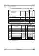
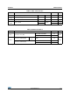
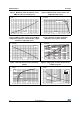
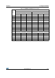
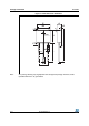
Table Of Contents
- Table 1. Main characteristics
- Table 2. Device summary
- 1 Characteristics
- Table 3. Absolute maximum ratings (Tj = 25 °C unless otherwise stated)
- Table 4. Electrical characteristics (Tj = 25 °C, unless otherwise stated)
- Table 5. Static characteristics
- Table 6. Thermal resistance
- Figure 1. Maximum power dissipation versus RMS on-state current (full cycle)
- Figure 2. RMS on-state current versus case temperature (full cycle)
- Figure 3. RMS on-state current versus ambient temperature (printed circuit board FR4, copper thickness: 35µm) (full cycle)
- Figure 4. Relative variation of thermal impedance versus pulse duration
- Figure 5. On-state characteristics (maximum values)
- Figure 6. Surge peak on-state current versus number of cycles
- Figure 7. Non-repetitive surge peak on-state current for a sinusoidal pulse with width tp < 10 ms and corresponding value of I2t
- Figure 8. Relative variation of gate trigger current, holding current and latching current versus junction temperature (typical values)
- Figure 9. Relative variation of critical rate of decrease of main current versus (dV/dt)c (typical values)
- Figure 10. Relative variation of critical rate of decrease of main current versus junction temperature
- Figure 11. DPAK thermal resistance junction to ambient versus copper surface under tab (printed circuit board FR4, copper thickness: 35 µm)
- 2 Package information
- Figure 12. DPAK dimension definitions
- Table 7. DPAK dimension values
- Figure 13. Footprint (dimensions in mm)
- Figure 14. ISOWATT220AB dimension definitions
- Table 8. ISOWATT220AB dimension values
- Figure 15. IPAK dimension definitions
- Table 9. IPAK dimension values
- Figure 16. TO-220AB (NIns. & Ins. 20-up) dimension definitions
- Table 10. TO-220AB (NIns. & Ins. 20-up) dimension values
- 3 Ordering information
- 4 Revision history

DocID7699 Rev 5 5/17
T4 series Characteristics
Figure 7. Non-repetitive surge peak on-state
current for a sinusoidal pulse with width t
p
< 10
ms and corresponding value of I
2
t
Figure 8. Relative variation of gate trigger
current, holding current and latching current
versus junction temperature (typical values)
0.01 0.10 1.00 10.00
1
10
100
500
I (A), I t (A s)
TSM
22
t (ms)
p
T initial=25°C
j
I
TSM
dI/dt limitation:
50A/µs
I t
2
-40 -20 0 20 40 60 80 100 120 140
0.0
0.5
1.0
1.5
2.0
2.5
T (°C)
j
I,I,I[T] /
GTHL j
I ,I ,I [T =25°C]
GTHL j
I
GT
I
H
& I
L
Figure 9. Relative variation of critical rate of
decrease of main current versus (dV/dt)c
(typical values)
Figure 10. Relative variation of critical rate of
decrease of main current versus junction
temperature
Figure 11. DPAK thermal resistance junction to ambient versus copper surface under tab (printed
circuit board FR4, copper thickness: 35 µm)
0.1 1.0 10.0 100.0
0.0
0.2
0.4
0.6
0.8
1.0
1.2
1.4
1.6
1.8
2.0
2.2
2.4
(dV/dt)c (V/µs)
(dI/dt)c [(dV/dt)c] / Specified (dI/dt)c
T405
T435
T410
0 25 50 75 100 125
0
1
2
3
4
5
6
(dI/dt)c [T ] / pecified]
j
(dI/dt)c [T s
j
T (°C)
j
0 4 8 1216202428323640
0
10
20
30
40
50
60
70
80
90
100
S(cm²)
R (°C/W)
th(j-a)