
Datasheet
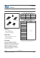
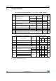
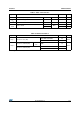
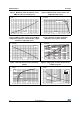
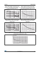
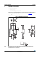
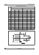
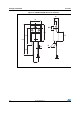
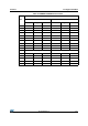
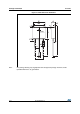
Table Of Contents
- Table 1. Main characteristics
- Table 2. Device summary
- 1 Characteristics
- Table 3. Absolute maximum ratings (Tj = 25 °C unless otherwise stated)
- Table 4. Electrical characteristics (Tj = 25 °C, unless otherwise stated)
- Table 5. Static characteristics
- Table 6. Thermal resistance
- Figure 1. Maximum power dissipation versus RMS on-state current (full cycle)
- Figure 2. RMS on-state current versus case temperature (full cycle)
- Figure 3. RMS on-state current versus ambient temperature (printed circuit board FR4, copper thickness: 35µm) (full cycle)
- Figure 4. Relative variation of thermal impedance versus pulse duration
- Figure 5. On-state characteristics (maximum values)
- Figure 6. Surge peak on-state current versus number of cycles
- Figure 7. Non-repetitive surge peak on-state current for a sinusoidal pulse with width tp < 10 ms and corresponding value of I2t
- Figure 8. Relative variation of gate trigger current, holding current and latching current versus junction temperature (typical values)
- Figure 9. Relative variation of critical rate of decrease of main current versus (dV/dt)c (typical values)
- Figure 10. Relative variation of critical rate of decrease of main current versus junction temperature
- Figure 11. DPAK thermal resistance junction to ambient versus copper surface under tab (printed circuit board FR4, copper thickness: 35 µm)
- 2 Package information
- Figure 12. DPAK dimension definitions
- Table 7. DPAK dimension values
- Figure 13. Footprint (dimensions in mm)
- Figure 14. ISOWATT220AB dimension definitions
- Table 8. ISOWATT220AB dimension values
- Figure 15. IPAK dimension definitions
- Table 9. IPAK dimension values
- Figure 16. TO-220AB (NIns. & Ins. 20-up) dimension definitions
- Table 10. TO-220AB (NIns. & Ins. 20-up) dimension values
- 3 Ordering information
- 4 Revision history

DocID7699 Rev 5 7/17
T4 series Package information
Figure 13. Footprint (dimensions in mm)
Table 7. DPAK dimension values
Ref.
Dimensions
Millimeters Inches
Min. Typ. Max. Min. Typ. Max.
A 2.18 2.40 0.086 0.094
A1 0.90 1.10 0.035 0.043
A2 0.03 0.23 0.001 0.009
b 0.64 0.90 0.025 0.035
b4 4.95 5.46 0.195 0.215
c 0.46 0.61 0.018 0.024
c2 0.46 0.60 0.018 0.023
D 5.97 6.22 0.235 0.244
D1 5.10 0.201
E 6.35 6.73 0.250 0.264
E1 4.32 0.170
e1 4.40 4.70 0.173 0.185
H 9.35 10.40 0.368 0.409
L 1.00 1.78 0.039 0.070
L2 1.27 0.05
L4 0.60 1.02 0.023 0.040
V2 0° 8° 0° 8°
6.7
6.7
3.03.0
1.6
5.094
A
B
The device must be positioned within
0.05 A B