
Datasheet
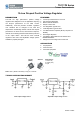

TS1117B Series
Taiwan Semiconductor
2 Version: H1607
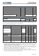
A
BSOLUTE
M
AXIMUM RATINGS
P
ARAMETER
S
YMBOL
L
IMIT
UNIT
Input Supply Voltage V
IN
15 V
Recommend Operation Input Supply Voltage V
IN (Opr. Typ.)
12 V
Power Dissipation (Note 2) P
D
Internal limited
Operating Temperature Range T
OPER
-40 ~ +125
o
C
Junction Temperature Range
T
J
+150
o
C
Storage Temperature Range
T
STG
-65 ~ +150
o
C
Lead Soldering Temperature (260
o
C)
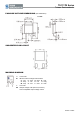
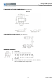
TO-252
5 s
SOT-223
THERMAL PERFORMANCE
PARAMETER SYMBOL
LIMIT
UNIT
SOT
-
223
TO
-
252
Junction to Ambient Thermal Resistance R
ӨJA
130 105 °C/W
Notes: R
ӨJA
is the sum of the junction-to-case and case-to-ambient thermal resistances. The case thermal reference is defined
at the solder mounting surface of the drain pins. R
ӨJA
is guaranteed by design while R
ӨCA
is determined by the user’s board
design. R
ӨJA
shown below for single device operation on FR-4 PCB in still air.
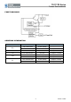
ELECTRICAL SPECIFICATIONS
(T
A
=25
o
C, unless otherwise noted)
PARAMETER
CONDITIONS
SYMBOL
M
IN
T
YP
M
AX
U
NIT
Reference Voltage
V
IN
= 2.75, I
O
=1A
V
REF
1.225
1.25 1.275
V
Output Voltage
(Note 4)
V
IN
= 2.7V~12V, I
O
=1A
V
OUT
1.176
1.2 1.224
V
V
IN
= 3V~12V, I
O
=1A 1.470
1.5 1.530
V
IN
= 4V~12V, I
O
=1A 2.450
2.5 2.550
V
IN
= 4.8V~12V, I
O
=1A 3.235
3.3 3.366
V
IN
= 6.5V~12V, I
O
=1A 4.900
5.0 5.100
Line Regulation V
O
+1.5V ≤ V
IN
≤ 12V, I
O
= 10mA REG
LINE
-- 0.2 0.5 %
Load Regulation
(Note 1,2)
V
IN
= V
OUT
+1.5V, I
O
= 10mA~1A REG
LOAD
-- 0.05 1.0 %
Dropout Voltage I
O
=1A, ∆V
OUT
= 1% V
OUT
V
DROP
-- 1.3 1.5 V
Quiescent Current V
IN
= 5V I
Q
-- 5 10 mA
Adjustable Pin Current I
ADJ
-- 90 -- µA
Output Current Limit V
IN
- V
OUT
= 1.5V I
LIMIT
1.1 -- -- A
Temperature Stability I
O
=10mA,
-- 0.5 -- %
Ripple Rejection
f= 120Hz, I
O
= 1A, C
OUT
=25µF,
V
IN
= V
OUT
+3V
RR -- 60 70 dB
Note:
1. See thermal regulation specification for changes in output voltage due to heating effects. Line and load
regulation are measured at a constant junction temperature by low duty cycle pulse testing. Load regulation is
measured at the output lead = 1/18” from the package.
2. Line and load regulation are guaranteed up to the maximum power dissipation of 15W. Power dissipation is
determined by the input / output voltage difference and the output current. Guaranteed maximum power
dissipation will not be available over the full input / output voltage range.
3. Quiescent current is defined as the minimum output current required to maintain the regulation.
4. The Output Capacitor does not have a theoretical upper limit and increasing its value will increase stability.
C
OUT
=100uF or more is typical for high current regulator design.