
Datasheet


TS431
Taiwan Semiconductor
Document Number: DS_P0000235 3 Version: H15
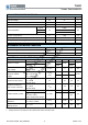
ORDERING INFORMATION
PART NO. PACKAGE PACKING
TS431ACT B0G
TO-92
1,000pcs / Bulk
TS431BCT B0G
TO-92
1,000pcs / Bulk
TS431ACT A3G
TO-92
2,000pcs / Ammo
TS431BCT A3G
TO-92
2,000pcs / Ammo
TS431ACX RFG
SOT-23 3,000pcs / 7” Reel
TS431BCX RFG
SOT-23 3,000pcs / 7” Reel
TS431ACS RLG
SOP-8 2,500pcs / 13” Reel
TS431BCS RLG SOP-8 2,500pcs / 13” Reel
TS431CS RLG SOP-8 2,500pcs / 13” Reel
Note:
1. Compliant to RoHS Directive 2011/65/EU and in accordance to WEEE 2002/96/EC.
2. Halogen-free according to IEC 61249-2-21 definition.
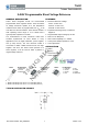
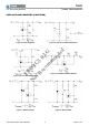
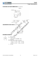
BLOCK DIAGRAM
* The deviation parameters ∆V
REF
and ∆I
REF
are defined as difference between the maximum value and minimum value
obtained over the full operating ambient temperature range that applied.
* The average temperature coefficient of the
reference input voltage, αV
REF
is defined as:
Where: T2-T1 = full temperature change.
αV
REF
can be positive or negative depending on whether the slope is positive or negative.
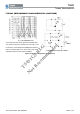
Example: Maximum V
REF
=2.496V at 30°C, minimum V
REF
=2.492V at 0°C, V
REF
=2.495V at 25°C, ΔT=70°C
αV
REF
| = [4mV / 2495mV] * 10
6
/ 70°C ≈ 23ppm/°C
Because minimum V
REF
occurs at the lower temperature, the coefficient is positive.
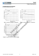
* The dynamic impedance ZKA is defined as:
| Z
KA
| = ΔV
KA
/ ΔI
KA
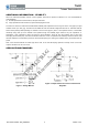
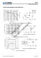
* When the device operating with two external resistors, R1 and R2, (refer to Figure 2) the total dynamic impedance of
the circuit is given by:
| Z
KA
| = Δv / Δi | ≈ Z
KA
| * ( 1 + R1 / R2)
TS431CS RLG
Not Recommended