
User's Manual
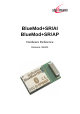


Table Of Contents
- 1 Introduction
- 2 Block Diagram
- 3 Application Interface
- 3.1 Power Supply
- 3.2 Power-up / -down Slew-Rate
- 3.3 Reset
- 3.4 Supply Voltage Monitor
- 3.5 Serial Interface
- 3.6 GPIO Interface
- 3.7 I2C Interface0F
- 3.8 SPI Serial Peripheral Interface1F
- 1.1
- 3.9 Bluetooth Radio Interface
- 3.10 WLAN Coexistence Interface2F
- 3.11 Slow Clock Interface
- 3.12 Test Mode Enable
- 3.13 Pin Strapped System Memory Boot Mode Invocation
- 3.14 Operating in a Power-Switched Environment
- 3.15 Serial Wire Interface
- 4 Module Pins
- 5 Electrical Characteristics
- 6 Mechanical Characteristics
- 1
- 7 Application Diagram
- 8 Approvals/Certifications
- 9 Related Documents
- 10 Packing
- 11 Ordering Information

BlueMod+SR/AI
BlueMod+SR/AP
Hardware Reference
Release r04d01 www.stollmann.de Page 3 of 65
Table of contents
1 Introduction .............................................................................................................................. 8
1.1 Feature Summary ............................................................................................................. 8
1.2 Applications ...................................................................................................................... 9
Support for any additional profile is possible on request........................................................... 9
1.2.1 General Cable Replacement ...................................................................................... 9
1.2.2 Industry ...................................................................................................................... 9
1.2.3 Automotive ................................................................................................................. 9
1.2.4 Healthcare and Medical ............................................................................................. 9
1.2.5 Sports and Fitness ................................................................................................... 10
1.2.6 Entertainment .......................................................................................................... 10
2 Block Diagram ....................................................................................................................... 11
3 Application Interface .............................................................................................................. 12
3.1 Power Supply ................................................................................................................. 12
3.2 Power-up / -down Slew-Rate .......................................................................................... 12
3.3 Reset .............................................................................................................................. 13
3.4 Supply Voltage Monitor ................................................................................................... 14
3.5 Serial Interface................................................................................................................ 15
3.5.1 3-Wire Serial Interface ............................................................................................. 16
3.5.2 Baudrate Deviation .................................................................................................. 17
3.6 GPIO Interface ................................................................................................................ 17
3.7 I
2
C Interface .................................................................................................................... 18
3.8 SPI Serial Peripheral Interface ........................................................................................ 19
3.9 Bluetooth Radio Interface ............................................................................................... 19
3.10 WLAN Coexistence Interface .......................................................................................... 20
3.11 Slow Clock Interface ....................................................................................................... 20
3.12 Test Mode Enable ........................................................................................................... 20
3.13 Pin Strapped System Memory Boot Mode Invocation ..................................................... 21
3.14 Operating in a Power-Switched Environment .................................................................. 21
3.15 Serial Wire Interface ....................................................................................................... 22
4 Module Pins ........................................................................................................................... 22
4.1 Pin Numbering ................................................................................................................ 22