
Datasheet

9
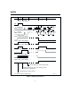
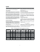
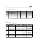
Absolute Maximum Ratings
Symbol Parameter Minimum Maximum Unit Notes
V
CC
V
CC
relative to V
SS
-0.3 +7.0 V
V
T
DC voltage applied on any pin ex
-
cluding V
CC
relative to V
SS
-0.3 +7.0 V
T
OPR
Operating ambient temperature -20 +70 °C Commercial
T
STG
Storage temperature -55 +125 °C
T
SOLDER
Soldering temperature - +260 °C 10 sec max.
T
BIAS
Temperature under bias -40 +85 °C
Note: Permanent device damage may occur if Absolute Maximum Ratings are exceeded. Functional opera
-
tion should be limited to the Recommended DC Operating Conditions detailed in this data sheet. Expo
-
sure to conditions beyond the operational limits for extended periods of time may affect device reliability.
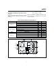
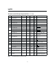
DC Thresholds (T
A
=T
OPR
;V
CC
±
10%)
Symbol Parameter Rating Tolerance Unit Notes
V
SNSHI
High threshold at SNS result-
ing in MOD = Low
0.05
*
V
CC
±
0.025
V
V
SNSLO
Low threshold at SNS result-
ing in MOD = High
0.04 * V
CC
±
0.025
V
V
LTF
Low-temperature fault
0.4
*
V
CC
±
0.030
V
V
TEMP
≥
V
LTF
inhib
-
its/terminates charge
V
HTF
High-temperature fault
(1/4
*
V
LTF
) + (3/4
*
V
TCO
)
±
0.030
V
V
TEMP
≤
V
HTF
inhibits
charge
V
EDV
End-of-discharge voltage
0.4
*
V
CC
±
0.030
V
V
CELL
<V
EDV
inhibits
fast charge
V
MCV
Maximum cell voltage
0.8
*
V
CC
±
0.030
V
V
CELL
>V
MCV
inhibits/
terminates charge
V
THERM
TS input change for∆T/∆t
detection
-16
±4
mV
V
CC
=5V,T
A
=25°C
-∆V
BAT input change for -∆V
detection
-12
±4
mV
V
CC
=5V,T
A
=25°C
PVD
BAT input change for PVD
detection
-6
±2
mV
V
CC
=5V,T
A
=25°C
bq2004