
Datasheet
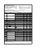
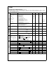
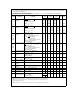
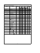

AC Electrical Specifications Test Conditions V
CC
e
4.5V and 5.5V (Unless Otherwise Specified) (Note 1)
Symbol Parameter Conditions
SBGRP 9 SBGRP 10 SBGRP 11
Units Notes
a
25
§
C
a
125
§
C
b
55
§
C
Min Max Min Max Min Max
f
C
e
CKI Freq. Operating Frequency 2 20 2 20 2 20 MHz (Note 5)
t
CI
e
1/FC Clock Period 50 50 50 ns (Note 5)
t
C
e
2/FC Timing Cycle 100 100 100 ns (Note 5)
t
LL
e
(/2 t
C
b
9 ALE Pulse Width 41 41 41 ns (Note 6)
t
ST
e
(/4 t
C
b
7 Address Valid to
18 18 18 ns (Note 6)
ALE Falling Edge
t
WAIT
e
t
C
e
WS Wait State Period 100 100 100 ns (Note 5)
FMW
e
0.0625 f
C
External MICROWIRE/PLUS
1.25 1.25 1.25 MHz (Note 6)
CLK Input Frequency
f
U
e
0.125 f
C
External UART
2.5 2.5 2.5 MHz (Note 5)
Clock Input Frequency
t
DCIC2
CK2 Delay From CK1 55 55 55 ns (Note 6)
t
ARR
e
(/4 t
C
b
5 ALE Falling Edge
20 20 20 ns (Note 6)
to RD
Falling Edge
t
RW
e
(/2 RD Pulse Width
140 140 140 ns (Note 6)
t
C
a
WS
b
10
t
DR
e
3.4 t
C
b
15 Data Hold after
0 60 0 60 0 60 ns (Note 6)
Rising Edge of RD
t
RD
e
(/2 RD Falling Edge to
85 85 85 ns (Note 6)
t
C
a
WS
b
65 Data in Valid
t
RDA
e
t
C
b
15 RD Rising Edge to
85 85 85 ns (Note 6)
Address Valid
t
VP
e
(/4 t
C
b
5 Address Hold from
20 20 20 ns (Note 6)
ALE Falling Edge
t
ARW
e
(/2 t
C
b
5 ALE Trailing Edge
45 45 45 ns (Note 6)
to WR
Falling Edge
t
WW
e
*/4 t
C
a
WS
b
15 WR Pulse Width 160 160 160 ns (Note 6)
t
HW
e
(/4 t
C
b
5 Data Hold after
20 20 20 ns (Note 6)
Trailing Edge of WR
t
V
e
(/2 t
C
a
WS
b
5 Data Valid before
145 145 145 ns (Note 6)
Rising Edge of WR
t
DAR
e
(/4 t
C
a
WS
b
50 Falling Edge of ALE
75 75 75 ns (Note 6)
to Falling Edge of RDY
10