
Datasheet
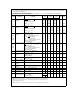

Absolute Maximum Ratings
If Military/Aerospace specified devices are required,
please contact the National Semiconductor Sales
Office/Distributors for availability and specifications.
Total Allowable Source or Sink Current 100 mA
Storage Temperature Range
b
65
§
Cto
a
150
§
C
Lead Temperature (Soldering, 10 sec) 300
§
C
V
CC
with Respect to GND
b
0.5V to 7.0V
All Other Pins (V
CC
a
0.5)V to (GND
b
0.5)V
Note:
Absolute maximum ratings indicate limits beyond
which damage to the device may occur. DC and AC electri-
cal specifications are not ensured when operating the de-
vice at absolute maximum ratings.
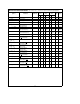
DC Electrical Characteristics V
CC
e
5.0V
g
10% unless otherwise specified, T
A
e
0
§
Cto
a
70
§
C for
HPC46083/HPC46003,
b
40
§
Cto
a
85
§
C for HPC36083/HPC36003,
b
40
§
Cto
a
105
§
C for
HPC26083/HPC26003,
b
55
§
Cto
a
125
§
C for HPC16083/HPC16003
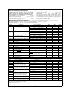
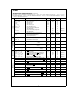
Symbol Parameter Test Conditions Min Max Units
I
CC
1
Supply Current V
CC
e
5.5V, f
in
e
30 MHz (Note 1) 65 mA
V
CC
e
5.5V, f
in
e
20 MHz (Note 1) 47 mA
V
CC
e
5.5V, f
in
e
2.0 MHz (Note 1) 10 mA
I
CC
2
IDLE Mode Current V
CC
e
5.5V, f
in
e
30 MHz (Note 1) 5.0 mA
V
CC
e
5.5V, f
in
e
20 MHz, (Note 1) 3.0 mA
V
CC
e
5.5V, f
in
e
2.0 MHz, (Note 1) 1 mA
I
CC
3
HALT Mode Current V
CC
e
5.5V, f
in
e
0 kHz, (Note 1) 200 mA
V
CC
e
2.5V, f
in
e
0 kHz, (Note 1) 50 mA
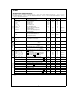
INPUT VOLTAGE LEVELS FOR SCHMITT TRIGGERED INPUTS RESET, NMI AND WO; AND ALSO CKI
V
IH
1
Logic High 0.9 V
CC
V
V
IL
1
Logic Low 0.1 V
CC
V
INPUT VOLTAGE LEVELS FOR ALL OTHER INPUTS
V
IH
2
Logic High 0.7 V
CC
V
V
IL
2
Logic Low 0.2 V
CC
V
I
LI1
Input Leakage Current V
IN
e
0 and V
IN
e
V
CC
g
2 mA
I
LI2
Input Leakage Current
V
IN
e
0
b
3
b
50 mA
RDY/HLD
, EXUI
I
LI3
Input Leakage Current
RESET
e
0, V
IN
e
V
CC
0.5 7 mA
B12
C
I
Input Capacitance (Note 2) 10 pF
C
IO
I/O Capacitance (Note 2) 20 pF
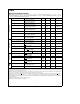
OUTPUT VOLTAGE LEVELS
V
OH
1
Logic High (CMOS) I
OH
eb
10 mA (Note 2) V
CC
b
0.1 V
V
OL
1
Logic Low (CMOS) I
OH
e
10 mA (Note 2) 0.1 V
V
OH
2
Port A/B Drive, CK2 I
OH
eb
7 mA 2.4 V
V
OL
2
(A
0
–A
15
,B
10
,B
11
,B
12
,B
15
)
I
OL
e
3 mA 0.4 V
V
OH
3
Other Port Pin Drive, WO (open I
OH
eb
1.6 mA (except WO) 2.4 V
V
OL
3
drain), (B
0
–B
9
,B
13
,B
14
,P
0
–P
3
)
I
OL
e
0.5 mA 0.4 V
V
OH4 ST1 and ST2 Drive I
OH
eb
6 mA 2.4 V
V
OL
4
I
OL
e
1.6 mA 0.4 V
V
OH5 Port A/B Drive (A
0
–A
15
,I
OH
eb
1 mA 2.4 V
B
10
,B
11
,B
12
,B
15
) when used
V
OL5
as External Address/Data Bus I
OL
e
3 mA 0.4 V
V
RAM
RAM Keep-Alive Voltage (Note 3) 2.5 V
CC
V
I
OZ
TRI-STATE
É
Leakage Current V
IN
e
0 and V
IN
e
V
CC
g
5 mA
Note 1: I
CC
1
,I
CC
2
,I
CC
3
measured with no external drive (I
OH
and I
OL
e
0, I
IH
and I
IL
e
0). I
CC
1
is measured with RESET
e
V
SS
,I
CC
3
is measured with NMI
e
V
CC
,
CKI driven to V
IH1
and V
IL1
, with rise and fall times less than 10 ns.
Note 2: This is guaranteed by design and not tested.
Note 3: Test duration is 100 ms.
2