
Datasheet

30 MHz
AC Electrical Characteristics
(See Notes 1 and 4 and
Figure 1
thru
Figure 5
)V
CC
e
5.0V
g
10% unless otherwise specified, T
A
e
0
§
Cto
a
70
§
C for
HPC46083/HPC46003,
b
40
§
Cto
a
85
§
C for HPC36083/HPC36003,
b
40
§
Cto
a
105
§
C for HPC26083/HPC26003,
b
55
§
Cto
a
125
§
C for HPC16083/HPC16003 (Continued)
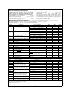
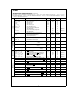
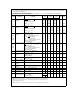
Symbol and Formula Parameter Min Max Units Notes
t
DC1ALER
Delay from CKI Rising Edge to ALE Rising Edge 0 35 ns (Notes 1, 2)
t
DC1ALEF
Delay from CKI Rising Edge to ALE Falling Edge 0 35 ns (Notes 1, 2)
t
DC2ALER
e
(/4 t
C
a
20 Delay from CK2 Rising Edge to ALE Rising Edge 37 ns (Note 2)
t
DC2ALEF
e
(/4 t
C
a
20 Delay from CK2 Falling Edge to ALE Falling Edge 37 ns (Note 2)
t
LL
e
(/2 t
C
b
9 ALE Pulse Width 24 ns
t
ST
e
(/4 t
C
b
7 Setup of Address Valid before ALE Falling Edge 9 ns
t
VP
e
(/4 t
C
b
5 Hold of Address Valid after ALE Falling Edge 11 ns
t
ARR
e
(/4 t
C
b
5 ALE Falling Edge to RD Falling Edge 12 ns
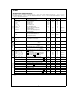
t
ACC
e
t
C
a
WS
b
32 Data Input Valid after Address Output Valid 100 ns (Note 6)
t
RD
e
(/2 t
C
a
WS
b
39 Data Input Valid after RD Falling Edge 60 ns
t
RW
e
(/2 t
C
a
WS
b
14 RD Pulse Width 85 ns
t
DR
e
*/4 t
C
b
15 Hold of Data Input Valid after RD Rising Edge 0 35 ns
t
RDA
e
t
C
b
15 Bus Enable after RD Rising Edge 51 ns
t
ARW
e
(/2 t
C
b
5 ALE Falling Edge to WR Falling Edge 28 ns
t
WW
e
*/4 t
C
a
WS
b
15 WR Pulse Width 101 ns
t
V
e
(/2 t
C
a
WS
b
5 Data Output Valid before WR
Rising Edge 94 ns
t
HW
e
(/4 t
C
b
10 Hold of Data Valid after WR Rising Edge 7 ns
t
DAR
e
(/4 t
C
a
WS
b
50 Falling Edge of ALE to Falling Edge of RDY 33 ns
t
RWP
e
t
C
RDY Pulse Width 66 ns
Address CyclesRead Cycles
Write
Cycles
Ready
Input
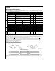
Note: C
L
e
40 pF.
Note 1: These AC characteristics are guaranteed with external clock drive on CKI having 50% duty cycle and with less than 15 pF load on CKO wih rise and fall
times (t
CKIR
and t
CKIL
) on CKI input less than 2.5 ns.
Note 2: Do not design with these parameters unless CKI is driven with an active signal. When using a passive crystal circuit, its stability is not guaranteed if either
CKI or CKO is connected to any external logic other than the passive components of the crystal circuit.
Note 3: t
HAE
is spec’d for case with HLD falling edge occurring at the latest time it can be accepted during the present CPU cycle being executed. If HLD falling
edge occurs later, t
HAE
as long as (3t
C
a
4WS
a
72 t
C
a
100) may occur depending on the following CPU instruction cycles, its wait states and ready input.
Note 4: WS t
WAIT
c
(number of pre-programmed wait states). Minimum and maximum values are calculated from maximum operating frequency, t
C
e
30 MHz,
with one wait state programmed.
Note 5: Due to emulation restrictionsÐactual limits will be better.
Note 6: This is guaranteed by design and not tested.
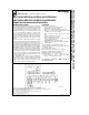
CKI Input Signal Characteristics
Rise/Fall Time
TL/DD/8801–35
Duty Cycle
TL/DD/8801–36
FIGURE 1. CKI Input Signal
TL/DD/8801–38
FIGURE 2. Input and Output for AC Tests
Note: AC testing inputs are driven at V
IH
for a logic ‘‘1’’ and V
IL
for a logic ‘‘0’’. Output timing measurements are made at 2.0V for a logic ‘‘1’’ and 0.8V for a logic
‘‘0’’.
6