
Datasheet

The following is the Military 883 Electrical Specification for HPC16083 and HPC16003. For latest information on RETS 16083X
contact NSC local sales office.
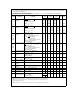
DC Electrical Specifications Test Conditions V
CC
e
5V
g
10% (Unless Otherwise Specified) (Note 1)
Symbol Parameter Conditions
SBGRP 1 SBGRP 2 SBGRP 3
Units Notes
a
25
§
C
a
125
§
C
b
55
§
C
Min Max Min Max Min Max
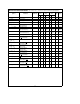
V
IH1
Logical ‘‘1’’ Input RESET, NMI, CKI and WO 0.9 0.9 0.9
V
Voltage B
10
–B
13
,B
15
(V
CC
)(V
CC
)(V
CC
)
V
IH2
All Inputs except Port A 0.7 0.7 0.7
V
(V
CC
)(V
CC
)(V
CC
)
V
IH3
Port A, V
CC
e
5.5V 4.65 4.65 4.65 V (Note 2)
Port A, V
CC
e
4.5V 3.95 3.95 3.95 V (Note 2)
V
IL1
Logical ‘‘0’’ Input RESET, NMI, CKI and WO 0.1 0.1 0.1
V
Voltage (V
CC
)(V
CC
)(V
CC
)
V
IL2
All Inputs except Port A 0.2 0.2 0.2
V
(V
CC
)(V
CC
)(V
CC
)
V
IL3
Port A, V
CC
e
5.5V 0.7 0.7 0.7 V (Note 3)
Port A, V
CC
e
4.5V 0.5 0.5 0.5 V (Note 3)
V
OH2
Logical ‘‘1’’ Output I
OH
eb
7mA(A
0
–A
15
,
2.4 2.4 2.4 V
Voltage B
10
–B
12
,B
15
, CK2)
V
OH3
I
OH3
eb
1.6 mA (B
0
–B
9
,B
13
–B
14
,
2.4 2.4 2.4 V
P
0
–P
3
), WO (Open Drain)
V
OH4
I
OH
eb
6 mA (ST1, ST2) 2.4 2.4 2.4 V
V
OH5
I
OH
eb
1mA(A
0
–A
15
,B
10
–B
12
,B
15
)
When Used as an External 2.4 2.4 2.4 V
Address/Data Bus
V
OL2
Logical ‘‘0’’ Output I
OL
e
3 mA (CK2, A
0
–A
15
,B
10
-B
12
,B
15
) 0.4 0.4 0.4 V
V
OL3
Voltage I
OL
e
0.5 mA (B
0
–B
9
,B
13
-B
14
,P
0
–P
3
0.4 0.4 0.4 V
WO (Open Drain)
V
OL4
I
OL
e
1.6 mA (ST1, ST2) 0.4 0.4 0.4 V
V
OL5
I
OL
e
3mA(A
0
–A
15
,B
10
–B
12
,B
15
)
When Used as an External 0.4 0.4 0.4 V
Address/Data Bus
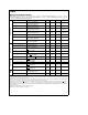
I
OZ
TRI-STATE Leakage V
SS
s
V
IN
s
V
CC
(WO, Port A,
g
5
g
5
g
5 mA
Port B), V
CC
e
5.5V
I
LI1
Input Leakage V
SS
s
V
IN
s
V
CC
,V
CC
e
5.5V
Current (I
1
–I
6
,D
0
–D
7
, CKI,
g
2
g
2
g
2 mA (Note 7)
RESET, EXM, EI)
I
LI2
Input Pullup Current V
IN
e
0(I
0
,I
7
, RDY/HLD,
b
50
b
3
b
50
b
3
b
50
b
3 mA (Note 7)
EXUI), V
CC
e
5.5V
I
LI3
Port B
12
Pulldown V
IN
e
V
CC
, Port B
12
,
171717mA
during Reset V
CC
e
5.5V
VRAM RAM Keep Alive Test Duration is 10 ms
2.5 2.5 2.5 V
Voltage
I
CC1
Supply Current F
IN
e
20 MHz, RESET
e
V
SS
,
55 55 55 mA
Dynamic I
OH
e
0 mA, I
OL
e
0 mA, V
CC
e
5.5V
I
CC2
Idle Mode Current F
IN
e
20 MHz, External Clock 3.5 3.5 3.5 mA
I
CC
Halt Mode Current NMI
e
V
CC
222mA
CI/O Input/Output f
test
e
1.0 MHz,
20 pF (Note 4)
Capacitance I/O Pin to Ground
SBGRP4
CI Input Capacitance f
test
e
1.0 MHz,
10 pF (Note 4)
Input Pin to Ground
Note 1: Electrical end point testing (when required) for GroupsC&Dshall consist only of subgroups 1, 2, 9 and 10.
Note 2: Port A V
IH
test limit includes 700 mV offset caused by output loads being on during Data Drive Time.
Note 3: Port A V
IL
test limit includes 400 mV offset caused by output loads being on during Data Drive Time.
Note 4: Verified at initial qual only.
Note 7: Future revisions of this device will not have pullups on pins I
0
,I
7
which will be tested to I
LI1
conditions.
9