
Datasheet

LM317L-N
www.ti.com
SNVS775J –MARCH 2000–REVISED MARCH 2013
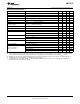
Electrical Characteristics
(1)
Parameter Conditions Min Typ Max Units
Line Regulation T
J
= 25°C, 3V ≤ (V
IN
− V
OUT
) ≤ 40V, I
L
≤ 20mA
(2)
0.01 0.04 %/V
Load Regulation T
J
= 25°C, 5mA ≤ I
OUT
≤ I
MAX
(2)
0.1 0.5 %
Thermal Regulation T
J
= 25°C, 10ms Pulse 0.04 0.2 %/W
Adjustment Pin Current 50 100 μA
Adjustment Pin Current 5mA ≤ I
L
≤ 100mA 0.2 5 μA
Change 3V ≤ (V
IN
− V
OUT
) ≤ 40V, P ≤ 625mW
3V ≤ (V
IN
− V
OUT
) ≤ 40V
(3)
1.20 1.25 1.30 V
Reference Voltage
5mA ≤ I
OUT
≤ 100mA, P ≤ 625mW
Line Regulation 3V ≤ (V
IN
− V
OUT
) ≤ 40V, I
L
≤ 20mA
(2)
0.02 0.07 %/V
Load Regulation 5mA ≤ I
OUT
≤ 100mA
(2)
0.3 1.5 %
Temperature Stability T
MIN
≤ T
J
≤ T
Max
0.65 %
Minimum Load Current (V
IN
− V
OUT
) ≤ 40V 3.5 5 mA
3V ≤ (V
IN
− V
OUT
) ≤ 15V 1.5 2.5
Current Limit 3V ≤ (V
IN
− V
OUT
) ≤ 13V 100 200 300 mA
(V
IN
− V
OUT
) = 40V 25 50 150 mA
Rms Output Noise, % of V
OUT
T
J
= 25°C, 10Hz ≤ f ≤ 10kHz 0.003 %
Ripple Rejection Ratio V
OUT
= 10V, f = 120Hz, C
ADJ
= 0 65 dB
C
ADJ
= 10μF 66 80 dB
Long-Term Stability T
J
= 125°C, 1000 Hours 0.3 1 %
Z Package 0.4″ Leads 180 °C/W
Z Package 0.125 Leads 160 °C/W
Junction to Ambient
Thermal Resistance
SOIC-8 Package 165 °C/W
6-DSBGA 290 °C/W
(1) Unless otherwise noted, these specifications apply: −25°C ≤ T
j
≤ 125°C for the LM317L-N; V
IN
− V
OUT
= 5V and I
OUT
= 40mA. Although
power dissipation is internally limited, these specifications are applicable for power dissipations up to 625mW. I
MAX
is 100mA.
(2) Regulation is measured at constant junction temperature, using pulse testing with a low duty cycle. Changes in output voltage due to
heating effects are covered under the specification for thermal regulation.
(3) Thermal resistance of the TO-92 package is 180°C/W junction to ambient with 0.4″ leads from a PC board and 160°C/W junction to
ambient with 0.125″ lead length to PC board.
Copyright © 2000–2013, Texas Instruments Incorporated Submit Documentation Feedback 3
Product Folder Links: LM317L-N