
Information


www.fastrongroup.com
Chip Inductors for RF Applications (Wire wound-open)Chip Inductors for RF Applications (Wire wound-open)
B
b
d1
d
D
Ko
T
Fig.2
Fig.1
P0
P
P1
W
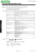
drawing only schematic, see table
Packing
Specification
•• All dimensions in mm
Revision date : 04 Sept 2013
Type Packing Code D d d1 B b W P P0 P1 Ko T Fig
0402 0
1, 08 180 60 13 12.7 8.4 8 2 4 2 0.6 - 2
0603 0
1, 08 180 60 13 12.7 8.4 8 4 4 2 1.0 0.25 1
0603 04 330 100 13 14.4 8.4 8 4 4 2 1.0 0.25 1
0805 0
1 180 60 13 12.7 8.4 8 4 4 2 1.63 0.25 1
0805 04 330 100 13 14.4 8.4 8 4 4 2 1.63 0.25 1
1008 01 180 60 13 12.7 8.4 8 4 4 2 2.23 0.3 1
1008 04 330 100 13 14.4 8.4 8 4 4 2 1.63 0.25 1
1206 01 180 60 13 12.7 8.4 8 4 4 2 1.8 0.2 1
1206 04 330 100 13 14.4 8.4 8 4 4 2 1.8 0.2 1
1210 01 180 60 13 18.4 13.7 12 8 4 2 2.55 0.3 1
1210 04 330 100 13 18.4 12.4 12 8 4 2 2.55 0.3 1
1812 01 180 60 13 18.4 13.7 12 8 4 2 3.70 0.35 1
1812 04 330 100 13 18.4 12.4 12 8 4 2 3.70 0.35 1
Ko
Packing Specification