
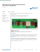
User Manual

UG:100 vicorpower.com Applications Engineering: 800 927.9474 Page 5
Theory of Operation
The schematic diagram is presented in functional blocks with text descriptions.
Component values are given in Bill of Materials, layout in PCB Layout (Figure 7).
So copies are available with download.
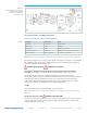
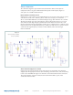
Input, Rectifier, and Filter Section
Input power is connected to screw terminal block J01. A 5 A fuse in F01 protects against
overcurrent. 330 W at 93% eciency draws 355W. At 85 V input, 4.17A is drawn.
Z01 is a 20 mm disk MOV that can withstand higher surges than Z02-Z04. R11 and R12
discharge the input capacitors when the line cord is pulled. Capacitors C15, C17-C20,
C24, and C25 return high frequency dierential current before it exits the line cord.
D01 through D04 form the input bridge rectifier. T01 is a high frequency common mode
inductor chosen for its high impedance up to 5 MHz. C01 and C03 are Y caps that return
common mode high frequency currents to GND (EARTH) rather than through
LINE or NEUTRAL.
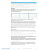
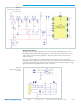
Active Transient Suppression Section
Input power enters from the filter at le. C24 and C01 are repeated in the schematic
snippet. Q01 through Q03 transistors turn o during a transient event, and can block up
to 200 V each. R04/R05 through to C22 form the control mechanism for the transistors.
T02 works with the capacitors inside the VI Brick® PFM® module as part of the
conducted emissions filter.
Figure 2.
Input, rectifier, and filter
section schematic