
User Manual

UG:100 vicorpower.com Applications Engineering: 800 927.9474 Page 7
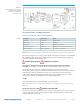
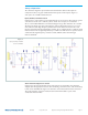
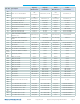
Output Filter Section
A common mode inductor should be used at the output to isolate switching noise from
this converter so it does not cause beat frequencies with downstream converters. The
one used in this reference design is the same used at the input so that a single part
number can be stocked. If space is at a premium, a smaller common mode inductor can
be substituted. Peak impedance should be between 500 kHz and 5 MHz.
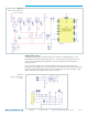
C37 is the bulk capacitor default on this board. Hold time will be increased roughly 50%
and power factor increased roughly 0.5% if a 10,000 uF capacitor is substituted. This
default capacitor is a 25 mm x 45 mm capacitor that is laid on its side. There are also two
2 mm holes, 10 mm spacing, which can be used for snap in type electrolytic capacitors.
Diameters up to 35 mm will clear other components on the PCB. This capacitor filters
the rectified line ripple, which is twice the input frequency. RMS ripple current rating
should be 80% of output current or higher for longer lifetime. Ripple current ratings
vary as a function of ambient temperature.
C30 through C34 are output ceramic filter capacitors. There are used to reduce the
switching ripple on the 48 V bus near 1 MHz. Screw terminal J02 or 0.100” spaced J03
can be used to connect output wires to the load or connect an external capacitor.
J12 is a probe socket with a local capacitor to reduce switching noise. R09 and R10 are
used to connect either the positive or negative output terminal to GND (EARTH). Only
one should be connected at a time. Both can be removed for a floating output.
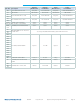
Figure 5.
Output filter section schematic