
Datasheet

1.5KE6.8A thru 1.5KE540A, 1N6267A thru 1N6303A
www.vishay.com
Vishay General Semiconductor
Revision: 22-Jan-14
3
Document Number: 88301
For technical questions within your region: DiodesAmericas@vishay.com
, DiodesAsia@vishay.com, DiodesEurope@vishay.com
THIS DOCUMENT IS SUBJECT TO CHANGE WITHOUT NOTICE. THE PRODUCTS DESCRIBED HEREIN AND THIS DOCUMENT
ARE SUBJECT TO SPECIFIC DISCLAIMERS, SET FORTH AT www.vishay.com/doc?91000
Note
(1)
AEC-Q101 qualified
RATINGS AND CHARACTERISTICS CURVES (T
A
= 25 °C unless otherwise noted)
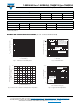
Fig. 1 - Peak Pulse Power Rating Curve
Fig. 2 - Pulse Power or Current vs. Initial Junction Temperature
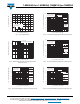
Fig. 3 - Pulse Waveform
Fig. 4 - Typical Junction Capacitance
THERMAL CHARACTERISTICS (T
A
= 25 °C unless otherwise noted)
PARAMETER SYMBOL VALUE UNIT
Typical thermal resistance, junction to ambient R
JA
75
Typical thermal resistance, junction to lead R
JL
15.4 °C/ W
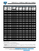
ORDERING INFORMATION (Example)
PREFERRED PIN UNIT WEIGHT (g) PREFERRED PACKAGE CODE BASE QUANTITY DELIVERY MODE
1.5KE6.8A-E3/54 0.968 54 1400 13" diameter paper tape and reel
1.5KE6.8AHE3/54
(1)
0.968 54 1400 13" diameter paper tape and reel
0.1
1
10
100
0.1 µs 1.0 µs 10 µs 100 µs 1.0 ms 10 ms
t
d
- Pulse Width (s)
P
PPM
- Peak Pulse Power (kW)
100
75
50
25
0
0 25 50 75 100 125 150 175 200
Peak Pulse P
ower (P
PP
) or Current (I
PP
)
Derating in Percentage, %
T
J
- Initial Temperature (°C)
0
50
100
150
t
r
= 10 µs
Peak Value
I
PPM
Half Value -
I
PPM
I
PP
2
t
d
10/1000 µs Waveform
as defined by R.E.A.
0
1.0
2.0
3.0 4.0
t - Time (ms)
I
PPM
- Peak Pulse Current, % I
RSM
T
J
= 25 °C
Pulse Width (t
d
)
is defined as the Point
where the Peak Current
decays to 50 % of I
PPM
5
10
100
500
10
100
1000
10 000
Uni-Directional
Bi-Directional
V
R
= 0
V
R
= Rated
Stand-Off Voltage
T
J
= 25 °C
f = 1.0 MHz
V
sig
= 50 mVp-p
V
BR
- Breakdown Voltage (V)
C
J
- Capacitance (pF)