
Datasheet

2W005G, 2W01G, 2W02G, 2W04G, 2W06G, 2W08G, 2W10G
www.vishay.com
Vishay General Semiconductor
Revision: 08-Jul-13
1
Document Number: 88528
For technical questions within your region: DiodesAmericas@vishay.com
, DiodesAsia@vishay.com, DiodesEurope@vishay.com
THIS DOCUMENT IS SUBJECT TO CHANGE WITHOUT NOTICE. THE PRODUCTS DESCRIBED HEREIN AND THIS DOCUMENT
ARE SUBJECT TO SPECIFIC DISCLAIMERS, SET FORTH AT www.vishay.com/doc?91000
Glass Passivated Single-Phase Bridge Rectifier
FEATURES
• UL recognition, file number E54214
• Ideal for printed circuit boards
• Typical I
R
less than 0.5 μA
• High case dielectric strength
• High surge current capability
• Solder dip 260 °C, 40 s
• Material categorization: For definitions of compliance
please see www.vishay.com/doc?99912
TYPICAL APPLICATIONS
General purpose use in AC/DC bridge full wave rectification
for power supply, adapter, charger, lighting ballaster on
consumers, and home appliances applications.
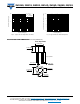
MECHANICAL DATA
Case: WOG
Molding compound meets UL 94 V-0 flammability rating
Base P/N-E4 - RoHS-compliant, commercial grade
Terminals: Silver plated leads, solderable per
J-STD-002 and JESD22-B102
Polarity: As marked on body
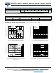
PRIMARY CHARACTERISTICS
Package WOG
I
F(AV)
2.0 A
V
RRM
50 V, 100 V, 200 V, 400 V, 600 V,
800 V, 1000 V
I
FSM
60 A
I
R
5 μA
V
F
at I
F
= 2.0 A 1.1 V
T
J
max. 150 °C
Diode variations Quad
Case Style WOG
+
−
~
~
+
−
~
~
e4
MAXIMUM RATINGS (T
A
= 25 °C unless otherwise noted)
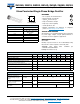
PARAMETER SYMBOL 2W005G 2W01G 2W02G 2W04G 2W06G 2W08G 2W10G UNIT
Maximum repetitive peak reverse voltage V
RRM
50 100 200 400 600 800 1000 V
Maximum RMS voltage V
RMS
35 70 140 280 420 560 700 V
Maximum DC blocking voltage V
DC
50 100 200 400 600 800 1000 V
Maximum average forward rectified current at
0.375" (9.5 mm) lead length at (fig. 1)
I
F(AV)
2.0 A
Peak forward surge current single half sine-wave
superimposed on rated load
I
FSM
60 A
Rating for fusing (t < 8.3 ms) I
2
t15A
2
s
Operating junction and storage temperature range T
J
, T
STG
- 55 to + 150 °C
ELECTRICAL CHARACTERISTICS (T
A
= 25 °C unless otherwise noted)
PARAMETER TEST CONDITIONS SYMBOL 2W005G 2W01G 2W02G 2W04G 2W06G 2W08G 2W10G UNIT
Maximum instantaneous
forward voltage drop per
diode
I
F
= 2.0 A V
F
1.1 V
Maximum DC reverse
current at rated DC blocking
voltage per diode
T
A
= 25 °C
I
R
5.0
μA
T
A
= 125 °C 500
Typical junction capacitance
per diode
4.0 V, 1 MHz C
J
40 20 pF