
Datasheet


Document Number: 83725 For technical questions, contact: optocoupler.answers@vishay.com
www.vishay.com
Rev. 1.5, 27-Feb-07 3
4N25/4N26/4N27/4N28
Optocoupler, Phototransistor Output,
with Base Connection
Vishay Semiconductors
Notes
(1)
T
amb
= 25 °C, unless otherwise specified.
Minimum and maximum values are testing requirements. Typical values are characteristics of the device and are the result of engineering
evaluation. Typical values are for information only and are not part of the testing requirements.
(2)
JEDEC registered values are 2500 V, 1500 V, 1500 V and 500 V for the 4N25, 4N26, 4N27 and 4N28 respectively.
Note
Indicates JEDEC registered values.
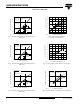
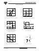
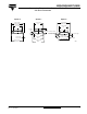
TYPICAL CHARACTERISTICS
T
amb
= 25 °C, unless otherwise specified
Fig. 1 - Forward Voltage vs. Forward Current
Fig. 2 - Normalized Non-Saturated and Saturated CTR vs.
LED Current
I
CBO
(dark)
(2)
V
CB
= 10 V,
(emitter open)
2.0 20 nA
Collector emitter capacitance V
CE
= 0 C
CE
6.0 pF
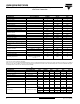
COUPLER
Isolation test voltage
(2)
Peak, 60 Hz V
IO
5300 V
Saturation voltage, collector emitter I
CE
= 2.0 mA, I
F
= 50 mA V
CE(sat)
0.5 V
Resistance, input output
(2)
V
IO
= 500 V R
IO
100 GΩ
Capacitance, input output f = 1 MHz C
IO
0.5 pF
CURRENT TRANSFER RATIO
PARAMETER TEST CONDITION PART SYMBOL MIN. TYP. MAX. UNIT
DC current transfer ratio V
CE
= 10 V, I
F
= 10 mA
4N25 CTR
DC
20 50 %
4N26 CTR
DC
20 50 %
4N27 CTR
DC
10 30 %
4N28 CTR
DC
10 30 %
SWITCHING CHARACTERISTICS
PARAMETER TEST CONDITION SYMBOL MIN. TYP. MAX. UNIT
Rise and fall times
V
CE
= 10 V, I
F
= 10 mA, R
L
= 100
Ω
t
r
, t
f
2.0 µs
ELECTRICAL CHARACTERISTICS
(1)
PARAMETER TEST CONDITION PART SYMBOL MIN. TYP. MAX. UNIT
i4n25_01
1001010.1
0.7
0.8
0.9
1.0
1.1
1.2
1.3
1.4
I
F
- Forward Current (mA)
V
F
-Forward Voltage (V)
T
A
= - 55 °C
T
A
= 25 °C
T
A
= 85 °C
i4n25_02
0.0
0.5
1.0
1.5
0 10 100
I
F
- LED Current (mA)
NCTR
NCTR(SAT)
NCTR - Normalized CTR
CTR
CE(sat)
= 0.4 V
V
CE
= 10 V, I
F
= 10 mA, T
A
= 25 °C
T
A
= 25 °C
Normalized to:
1