
Datasheet

BAS381, BAS382, BAS383
www.vishay.com
Vishay Semiconductors
Rev. 2.2, 02-Jun-17
3
Document Number: 85503
For technical questions within your region: DiodesAmericas@vishay.com
, DiodesAsia@vishay.com, DiodesEurope@vishay.com
THIS DOCUMENT IS SUBJECT TO CHANGE WITHOUT NOTICE. THE PRODUCTS DESCRIBED HEREIN AND THIS DOCUMENT
ARE SUBJECT TO SPECIFIC DISCLAIMERS, SET FORTH AT www.vishay.com/doc?91000
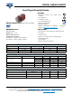
Fig. 5 - Board for R
thJA
Definition (in mm)
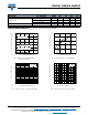
PACKAGE DIMENSIONS in millimeters (inches): MicroMELF
25
2.5
10
0.71 1.3
1.27
9.9
24
0.152
0.355
95 10329
Cathode indification
surface plan1 (0.039)
glass
glass
surface plan
2 (0.079)
1.8 (0.071)
0.25 (0.010)
0.15 (0.006)
1.2 (0.047)
1.1 (0.043)
> R2.5 (0.098)
< 1.35 (0.053)
0.6 (0.024)
Foot print recommendation:
Reflow soldering Wave soldering
2.4 (0.094) 2.8 (0.110)
0.8 (0.031)0.8 (0.031) 0.9 (0.035) 0.9 (0.035)
1.2 (0.047)
0.8 (0.031)
1.4 (0.055)
1 (0.039)
Document no.:6.560-5007.01-4
Rev. 13 - Date: 07.June.2006
96 12072
Created - Date: 26.July.1996
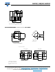
*
*
The gap between plug and glass can
be either on cathode or anode side