
Datasheet

BYS12-90-M3
www.vishay.com
Vishay General Semiconductor
Revision: 09-May-2019
3
Document Number: 89412
For technical questions within your region: DiodesAmericas@vishay.com
, DiodesAsia@vishay.com, DiodesEurope@vishay.com
THIS DOCUMENT IS SUBJECT TO CHANGE WITHOUT NOTICE. THE PRODUCTS DESCRIBED HEREIN AND THIS DOCUMENT
ARE SUBJECT TO SPECIFIC DISCLAIMERS, SET FORTH AT www.vishay.com/doc?91000
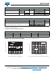
Fig. 3 - Max. Average Forward Current vs. Ambient Temperature
Fig. 4 - Reverse Current vs. Junction Temperature
Fig. 5 - Max. Reverse Power Dissipation vs. Junction Temperature
Fig. 6 - Diode Capacitance vs. Reverse Voltage
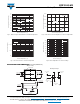
PACKAGE OUTLINE DIMENSIONS in inches (millimeters)
V
R
= 0 V, Half Sine-Wave
R
thJL
= 25 K/W
100 K/W
125 K/W
150 K/W
2.0
1.6
1.2
0.8
0.4
0
0 40 80 120 160 200
Ambient Temperature (°C)
Average Forward Current (A)
2.2
1.8
1.4
1.0
0.6
0.2
100 000
10 000
1000
100
25 50 75 100 125 150
Reverse Current (µA)
Junction Temperature (°C)
V
R
= V
RRM
2500
2000
1500
1000
500
0
25 50 75 100 125 150
V
R
= V
RRM
P
R
- Limit
at 100 % V
R
Reverse Power Dissipation (mW)
Junction Temperature (°C)
180
160
140
120
100
80
60
40
20
0
0.1 1 10 100
f = 1 MHz
Reverse Voltage (V)
Diode Capacitance (pF)
0.008 (0.203)
0.194 (4.93)
0.208 (5.28)
0.157 (3.99)
0.177 (4.50)
0.100 (2.54)
0.110 (2.79)
0.078 (1.98)
0.090 (2.29)
0.006 (0.152)
0.012 (0.305)
0.049 (1.25)
0.065 (1.65)
Cathode Band
0 (0)
SMA (DO-214AC)
Mounting Pad Layout
0.074 (1.88)
MAX.
0.208 (5.28)
REF.
0.066 (1.68)
MIN.
0.060 (1.52)
MIN.
0.030 (0.76)
0.060 (1.52)