
Datasheet

CNY17F
www.vishay.com
Vishay Semiconductors
Rev. 2.2, 08-Jan-14
2
Document Number: 83607
For technical questions, contact: optocoupleranswers@vishay.com
THIS DOCUMENT IS SUBJECT TO CHANGE WITHOUT NOTICE. THE PRODUCTS DESCRIBED HEREIN AND THIS DOCUMENT
ARE SUBJECT TO SPECIFIC DISCLAIMERS, SET FORTH AT www.vishay.com/doc?91000
Notes
• Stresses in excess of the absolute maximum ratings can cause permanent damage to the device. Functional operation of the device is not
implied at these or any other conditions in excess of those given in the operational sections of this document. Exposure to absolute
maximum ratings for extended periods of the time can adversely affect reliability.
(1)
Refer to reflow profile for soldering conditions for surface mounted parts (SMD). Refer to wave profile for soldering conditions for through
hole parts (DIP).
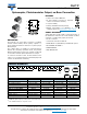
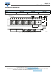
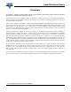
Fig. 1 - Total Power Dissipation vs. Ambient Temperature
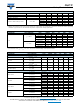
ABSOLUTE MAXIMUM RATINGS (T
amb
= 25 °C, unless otherwise specified)
PARAMETER TEST CONDITION SYMBOL VALUE UNIT
INPUT
Reverse voltage V
R
6V
DC forward current I
F
60 mA
Surge forward current t ≤ 10 μs I
FSM
2.5 A
Power dissipation P
diss
100 mW
OUTPUT
Collector emitter breakdown voltage BV
CEO
70 V
Collector current I
C
50 mA
Collector peak current t
p
/T = 0.5, t
p
≤ 10 ms I
CM
100 mA
Output power dissipation P
diss
150 mW
COUPLER
Isolation test voltage between emitter and
detector
t = 1 min V
ISO
5000 V
RMS
Storage temperature range T
stg
-55 to +150 °C
Ambient temperature range T
amb
-55 to +110 °C
Junction temperature T
j
100 °C
Soldering temperature
(1)
2 mm from case, ≤ 10 s T
sld
260 °C
Total power dissipation P
diss
250 mW
ELECTRICAL CHARACTERISTICS (T
amb
= 25 °C, unless otherwise specified)
PARAMETER TEST CONDITION PART SYMBOL MIN. TYP. MAX. UNIT
INPUT
Forward voltage I
F
= 60 mA V
F
1.39 1.65 V
Breakdown voltage I
R
= 10 μA V
BR
6V
Reverse current V
R
= 6 V I
R
0.01 10 μA
Capacitance V
R
= 0 V, f = 1 MHz C
O
25 pF
OUTPUT
Collector emitter capacitance V
CE
= 5 V, f = 1 MHz C
CE
5.2 pF
Base collector capacitance V
CE
= 5 V, f = 1 MHz C
BC
6.5 pF
Emitter base capacitance V
CE
= 5 V, f = 1 MHz C
EB
7.5 pF
0
50
100
150
200
250
300
0 20 40 60 80 100 120
P
tot
- Total Power Dissipation (mW)
T
amb
- Ambient Temperature (°C)
Coupled device
Phototransistor
IR-diode