
Datasheet

www.vishay.com For technical questions, contact: optocoupleranswers@vishay.com
Document Number: 83526
2 Rev. 1.9, 20-Oct-09
CNY74-2H, CNY74-4H
Vishay Semiconductors
Optocoupler, Phototransistor Output
(Multichannel)
Note
T
amb
= 25 °C, unless otherwise specified.
Stresses in excess of the absolute maximum ratings can cause permanent damage to the device. Functional operation of the device is not implied
at these or any other conditions in excess of those given in the operational sections of this document. Exposure to absolute maximum ratings for
extended periods of the time can adversely affect reliability.
Note
T
amb
= 25 °C, unless otherwise specified.
Minimum and maximum values are testing requirements. Typical values are characteristics of the device and are the result of engineering
evaluation. Typical values are for information only and are not part of the testing requirements.
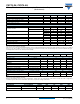
OUTPUT
Collector emitter breakdown voltage BV
CEO
70 V
Emitter collector breakdown voltage BV
ECO
7V
Power dissipation P
diss
150 mW
Derate linearly from 25 °C 2mW/°C
COUPLER
Isolation test voltage t = 1 s V
ISO
5300 V
RMS
Isolation resistance
V
IO
= 500 V, T
amb
= 25 °C R
IO
≥ 10
12
Ω
V
IO
= 500 V, T
amb
= 100 °C R
IO
≥ 10
11
Ω
Total package dissipation
CNY74-2H P
tot
400 mW
CNY74-4H P
tot
500 mW
Derate linearly from 25 °C
CNY74-2H 5.33 mW/°C
CNY74-4H 6.67 mW/°C
Creepage distance ≥ 7mm
Clearance distance ≥ 7mm
Storage temperature T
stg
- 55 to + 150 °C
Operating temperature T
amb
- 55 to + 100 °C
Lead soldering time at 260 °C 10 s
ABSOLUTE MAXIMUM RATINGS
PARAMETER TEST CONDITION PART SYMBOL VALUE UNIT
ELECTRICAL CHARACTERISTICS
PARAMETER TEST CONDITION SYMBOL MIN. TYP. MAX. UNIT
INPUT
Forward voltage I
F
= 20 mA V
F
1.3 1.5 V
Reverse current V
R
= 3 V I
R
0.1 100 µA
Capacitance V
R
= 0 V C
O
25 pF
OUTPUT
Collector emitter breakdown voltage I
C
= 1 mA BV
CEO
70 V
Collector emitter leakage current V
CE
= 5 V, I
F
= 0 A I
CEO
100 nA
Capacitance collector emitter V
CE
= 0 V, f = 1 Hz C
CE
10 pF
COUPLER
Saturation voltage, collector emitter I
C
= 2 mA, I
F
= 16 mA V
CEsat
0.3 0.5 V
Resistance (input to output) R
IO
100 GΩ
Capacitance (input to output) C
IO
0.5 pF
CURRENT TRANSFER RATIO
PARAMETER TEST CONDITION SYMBOL MIN. TYP. MAX. UNIT
DC current transfer ratio I
F
= 5 mA, V
CE
= 5 V CTR 50 600 %
DC current transfer ratio I
F
= 10 mA, V
CE
= 5 V CTR 60 %