
Datasheet

Document Number: 83526 For technical questions, contact: optocoupleranswers@vishay.com
www.vishay.com
Rev. 1.9, 20-Oct-09 3
CNY74-2H, CNY74-4H
Optocoupler, Phototransistor Output
(Multichannel)
Vishay Semiconductors
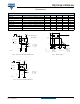
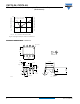
Fig. 1 - Test Circuit, Non-Saturated Operation
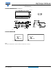
Fig. 2 - Test Circuit, Saturated Operation
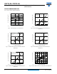
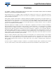
Fig. 3 - Switching Times
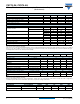
SWITCHING CHARACTERISTICS
PARAMETER TEST CONDITION SYMBOL MIN. TYP. MAX. UNIT
Delay time V
S
= 5 V, I
C
= 2 mA, R
L
= 100 Ω (see figure 1) t
d
3µs
Rise time V
S
= 5 V, I
C
= 2 mA, R
L
= 100 Ω (see figure 1) t
r
3µs
Fall time V
S
= 5 V, I
C
= 2 mA, R
L
= 100 Ω (see figure 1) t
f
4.7 µs
Storage time V
S
= 5 V, I
C
= 2 mA, R
L
= 100 Ω (see figure 1) t
s
0.3 µs
Turn-on time V
S
= 5 V, I
C
= 2 mA, R
L
= 100 Ω (see figure 1) t
on
6µs
Turn-off time V
S
= 5 V, I
C
= 2 mA, R
L
= 100 Ω (see figure 1) t
off
5µs
Turn-on time V
S
= 5 V, I
C
= 10 mA, R
L
= 1 kΩ (see figure 2) t
on
9µs
Turn-off time V
S
= 5 V, I
C
= 10 mA, R
L
= 1 kΩ (see figure 2) t
off
18 µs
Channel I
Channel II
95 10804
R
G
= 50 Ω
t
p
t
p
= 50 µs
T
= 0.01
+ 5 V
I
F
0
50 Ω 100 Ω
I
F
I
C
= 2 mA; adjusted through
input amplitude
Oscilloscope
R
L
= 1 MΩ
C
L
= 20 pF
Channel I
Channel II
95 10843
R
G
= 50 Ω
t
p
t
p
= 50 µs
T
= 0.01
+ 5 V
I
C
I
F
0
50 Ω
1 kΩ
I
F
= 10 mA
Oscilloscope
R
L
≥
C
L
20 pF
1 MΩ
≤
t
p
t
t
0
0
10 %
90 %
100 %
t
r
t
d
t
on
t
s
t
f
t
off
I
F
I
C
t
p
Pulse duration
t
d
Delay time
t
r
Rise time
t
on
(= t
d
+ t
r
) Turn-on time
t
s
Storage time
t
f
Fall time
t
off
(= t
s
+ t
f
)Turn-off time
96 11698