
Datasheet


Document Number: 83536 For technical questions, contact: optocoupleranswers@vishay.com
www.vishay.com
Rev. 2.0, 28-Oct-09 255
CNY75A, CNY75B, CNY75C, CNY75GA, CNY75GB, CNY75GC
Optocoupler, Phototransistor Output,
with Base Connection
Vishay Semiconductors
Notes
(1)
T
amb
= 25 °C, unless otherwise specified.
Stresses in excess of the absolute maximum ratings can cause permanent damage to the device. Functional operation of the device is not
implied at these or any other conditions in excess of those given in the operational sections of this document. Exposure to absolute maximum
ratings for extended periods of the time can adversely affect reliability.
(2)
Refer to wave profile for soldering conditions for through hole devices.
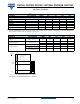
Note
(1)
T
amb
= 25 °C, unless otherwise specified.
Minimum and maximum values were tested requierements. Typical values are characteristics of the device and are the result of engineering
evaluations. Typical values are for information only and are not part of the testing requirements.
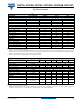
ABSOLUTE MAXIMUM RATINGS
(1)
PARAMETER TEST CONDITION SYMBOL VALUE UNIT
INPUT
Reverse voltage V
R
5V
Forward current I
F
60 mA
Forward surge current t
p
≤ 10 µs I
FSM
3A
Power dissipation P
diss
70 mW
Junction temperature T
j
125 °C
OUTPUT
Collector base voltage V
CBO
70 V
Collector emitter voltage V
CEO
70 V
Emitter collector voltage V
ECO
7V
Collector current I
C
50 mA
Collector peak current t
p
/T = 0.5, t
p
≤ 10 ms I
CM
100 mA
Power dissipation P
diss
70 mW
Junction temperature T
j
125 °C
COUPLER
AC isolation test voltage (RMS) V
ISO
5000 V
RMS
Total power dissipation P
tot
200 mW
Ambient temperature range T
amb
- 55 to + 110 °C
Storage temperature range T
stg
- 55 to + 125 °C
Soldering temperature
(2)
2 mm from case, t ≤ 10 s T
sld
260 °C
ELECTRICAL CHARACTERISTCS
(1)
PARAMETER TEST CONDITION PART SYMBOL MIN. TYP. MAX. UNIT
INPUT
Forward voltage I
F
= 50 mA V
F
1.25 1.6 V
Reverse current V
R
= 6 V I
R
10 µA
Junction capacitance V
R
= 0 V, f = 1 MHz C
j
50 pF
OUTPUT
Collector base voltage I
C
= 100 µA V
CBO
70 V
Collector emitter voltage I
C
= 1 mA V
CEO
70 V
Emitter collector voltage I
E
= 100 µA V
ECO
7V
Collector emitter leakage current V
CE
= 20 V, I
F
= 0 A I
CEO
150 nA
COUPLER
Collector emitter saturation voltage I
F
= 10 mA, I
C
= 1 mA V
CEsat
0.3 V
Cut-off frequency
V
CE
= 5 V, I
F
= 10 mA,
R
L
= 100 Ω
f
c
110 kHz
Coupling capacitance f = 1 MHz C
k
0.6 pF