
Datasheet

IL420, IL4208
www.vishay.com
Vishay Semiconductors
Rev. 2.1, 11-Jun-13
2
Document Number: 83629
For technical questions, contact: optocoupleranswers@vishay.com
THIS DOCUMENT IS SUBJECT TO CHANGE WITHOUT NOTICE. THE PRODUCTS DESCRIBED HEREIN AND THIS DOCUMENT
ARE SUBJECT TO SPECIFIC DISCLAIMERS, SET FORTH AT www.vishay.com/doc?91000
Notes
• Stresses in excess of the absolute maximum ratings can cause permanent damage to the device. Functional operation of the device is not
implied at these or any other conditions in excess of those given in the operational sections of this document. Exposure to absolute
maximum ratings for extended periods of the time can adversely affect reliability.
(1)
Refer to reflow profile for soldering conditions for surface mounted devices (SMD). Refer to wave profile for soldering condditions for through
hole devices (DIP).
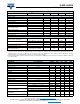
ABSOLUTE MAXIMUM RATINGS (T
amb
= 25 °C, unless otherwise specified)
PARAMETER TEST CONDITION PART SYMBOL VALUE UNIT
INPUT
Reverse voltage V
R
6V
Forward current I
F
60 mA
Surge current I
FSM
2.5 A
Power dissipation P
diss
100 mW
Derate from 25 °C 1.33 mW/°C
OUTPUT
Peak off-state voltage
IL420 V
DRM
600 V
IL4208 V
DRM
800 V
RMS on-state current I
TM
300 mA
Single cycle surge current I
TSM
3A
Power dissipation P
diss
500 mW
Derate from 25 °C 6.6 mW/°C
COUPLER
Isolation test voltage
between emitter and detector
t = 1 s V
ISO
5300 V
RMS
Isolation resistance
V
IO
= 500 V, T
amb
= 25 °C R
IO
10
12
V
IO
= 500 V, T
amb
= 100 °C R
IO
10
11
Storage temperature range T
stg
- 55 to + 150 °C
Ambient temperature range T
amb
- 55 to + 100 °C
Soldering temperature
(1)
max. 10 s dip soldering
0.5 mm from case bottom
T
sld
260 °C
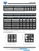
ELECTRICAL CHARACTERISTICS (T
amb
= 25 °C, unless otherwise specified)
PARAMETER TEST CONDITION SYMBOL MIN. TYP. MAX. UNIT
INPUT
Forward voltage I
F
= 10 mA V
F
1.16 1.35 V
Reverse current V
R
= 6 V I
R
0.1 10 μA
Input capacitance V
F
= 0 V, f = 1 MHz C
IN
40 pF
Thermal resistance, junction to ambient R
thja
750 °C/W
OUTPUT
Off-state current V
D
= V
DRM
, T
amb
= 100 °C I
DRM
10 100 μA
On-state voltage I
T
= 300 mA V
TM
1.7 3 V
Surge (non-repetitive), on-state current f = 50 Hz I
TSM
3A
Holding current I
H
65 500 μA
Latching current V
T
= 2.2 V I
L
500 μA
LED trigger current V
D
= 5 V I
FT
12mA
Trigger current temperature gradient I
FT
/T
j
714μA/°C
Critical rate of rise off-state voltage
V
D
= 0.67 V
DRM
, T
j
= 25 °C dV/dt
cr
10 000 V/μs
V
D
= 0.67 V
DRM
, T
j
= 80 °C dV/dt
cr
5000 V/μs
Critical rate of rise of voltage
at current commutation
V
D
= 230 V
RMS
, I
D
= 300 mA
RMS
, T
J
= 25 °C dV/dt
crq
8V/μs
V
D
= 230 V
RMS
, I
D
= 300 mA
RMS
, T
J
= 85 °C dV/dt
crq
7V/μs
Critical rate of rise of on-state current
commutation
dI/dt
crq
12 A/ms
Thermal resistance, junction to ambient R
thja
150 °C/W