
Datasheet

Document Number: 91034 www.vishay.com
S11-0509-B, 21-Mar-11 7
This datasheet is subject to change without notice.
THE PRODUCT DESCRIBED HEREIN AND THIS DATASHEET ARE SUBJECT TO SPECIFIC DISCLAIMERS, SET FORTH AT
www.vishay.com/doc?91000
IRF634, SiHF634
Vishay Siliconix
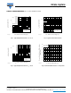
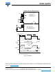
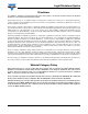
Fig. 14 - For N-Channel
Vishay Siliconix maintains worldwide manufacturing capability. Products may be manufactured at one of several qualified locations. Reliability data for Silicon
Technology and Package Reliability represent a composite of all qualified locations. For related documents such as package/tape drawings, part marking, and
reliability data, see www.vishay.com/ppg?91034
.
P.W.
Period
dI/dt
Diode recovery
dV/dt
Ripple ≤ 5 %
Body diode forward drop
Re-applied
voltage
Reverse
recovery
current
Body diode forward
current
V
GS
= 10 V
a
I
SD
Driver gate drive
D.U.T. l
SD
waveform
D.U.T. V
DS
waveform
Inductor current
D =
P.W.
Period
+
-
+
+
+
-
-
-
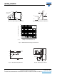
Peak Diode Recovery dV/dt Test Circuit
V
DD
• dV/dt controlled by R
g
• Driver same type as D.U.T.
•
I
SD
controlled by duty factor “D”
• D.U.T. - device under test
D.U.T.
Circuit layout considerations
• Low stray inductance
• Ground plane
• Low leakage inductance
current transformer
R
g
Note
a. V
GS
= 5 V for logic level devices
V
DD