
Datasheet

www.vishay.com Document Number: 91067
2 S11-0506-Rev. B, 21-Mar-11
This datasheet is subject to change without notice.
THE PRODUCT DESCRIBED HEREIN AND THIS DATASHEET ARE SUBJECT TO SPECIFIC DISCLAIMERS, SET FORTH AT
www.vishay.com/doc?91000
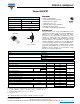
IRF840LC, SiHF840LC
Vishay Siliconix
Notes
a. Repetitive rating; pulse width limited by maximum junction temperature (see fig. 11).
b. Pulse width ≤ 300 μs; duty cycle ≤ 2 %.
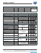
THERMAL RESISTANCE
PARAMETER SYMBOL TYP. MAX. UNIT
Maximum Junction-to-Ambient R
thJA
-62
°C/WCase-to-Sink, Flat, Greased Surface R
thCS
0.50 -
Maximum Junction-to-Case (Drain) R
thJC
-1.0
SPECIFICATIONS (T
J
= 25 °C, unless otherwise noted)
PARAMETER SYMBOL TEST CONDITIONS MIN. TYP. MAX. UNIT
Static
Drain-Source Breakdown Voltage V
DS
V
GS
= 0 V, I
D
= 250 μA 500 - - V
V
DS
Temperature Coefficient
ΔV
DS
/T
J
Reference to 25 °C, I
D
= 1 mA
-0.63-
V/°C
Gate-Source Threshold Voltage V
GS(th)
V
DS
= V
GS
, I
D
= 250 μA 2.0 - 4.0 V
Gate-Source Leakage I
GSS
V
GS
= ± 20 V - - ± 100 nA
Zero Gate Voltage Drain Current I
DSS
V
DS
= 500 V, V
GS
= 0 V - - 25
μA
V
DS
= 400V, V
GS
= 0 V, T
J
= 125 °C - - 250
Drain-Source On-State Resistance R
DS(on)
V
GS
= 10 V I
D
= 4.8 A
b
- - 0.85 Ω
Forward Transconductance g
fs
V
DS
= 50 V, I
D
= 4.8 A
b
4.0 - - S
Dynamic
Input Capacitance C
iss
V
GS
= 0 V,
V
DS
= 25 V,
f = 1.0 MHz, see fig. 5
-1100-
pFOutput Capacitance C
oss
-170-
Reverse Transfer Capacitance C
rss
-18-
Total Gate Charge Q
g
V
GS
= 10 V
I
D
= 8.0 A, V
DS
= 400 V
see fig. 6 and 13
b
--39
nC Gate-Source Charge Q
gs
--10
Gate-Drain Charge Q
gd
--19
Turn-On Delay Time t
d(on)
V
DD
= 250 V, I
D
= 8.0 A,
R
g
= 9.1 Ω, R
D
= 30 Ω
see fig. 10
b
-12-
ns
Rise Time t
r
-25-
Turn-Off Delay Time t
d(off)
-27-
Fall Time t
f
-19-
Internal Drain Inductance L
D
Between lead,
6 mm (0.25") from
package and center of
die contact
-4.5-
nH
Internal Source Inductance L
S
-7.5-
Drain-Source Body Diode Characteristics
Continuous Source-Drain Diode Current I
S
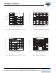
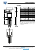
MOSFET symbol
showing the
integral reverse
p - n junction diode
--8.0
A
Pulsed Diode Forward Current
a
I
SM
--28
Body Diode Voltage V
SD
T
J
= 25 °C, I
S
= 8.0 A, V
GS
= 0 V
b
--2.0V
Body Diode Reverse Recovery Time t
rr
T
J
= 25 °C, I
F
= 8.0 A,
dI/dt = 100 A/μs
b
- 490 740 ns
Body Diode Reverse Recovery Charge Q
rr
-3.04.5μC
Forward Turn-On Time t
on
Intrinsic turn-on time is negligible (turn-on is dominated by L
S
and L
D
)
D
S
G
S
D
G