
Datasheet

www.vishay.com Document Number: 91067
4 S11-0506-Rev. B, 21-Mar-11
This datasheet is subject to change without notice.
THE PRODUCT DESCRIBED HEREIN AND THIS DATASHEET ARE SUBJECT TO SPECIFIC DISCLAIMERS, SET FORTH AT
www.vishay.com/doc?91000
IRF840LC, SiHF840LC
Vishay Siliconix
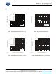
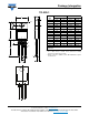
Fig. 5 - Typical Capacitance vs. Drain-to-Source Voltage
Fig. 6 - Typical Gate Charge vs. Gate-to-Source Voltage
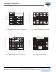
Fig. 7 - Typical Source-Drain Diode Forward Voltage
Fig. 8 - Maximum Safe Operating Area
2400
2000
1600
1200
0
400
800
10
0
10
1
Capacitance (pF)
V
DS
,
Drain-to-Source Voltage (V)
C
iss
C
rss
C
oss
V
GS
= 0 V, f = 1 MHz
C
iss
= C
gs
+ C
gd
, C
ds
Shorted
C
rss
= C
gd
C
oss
= C
ds
+ C
gd
91067_05
Q
G
, Total Gate Charge (nC)
V
GS
, Gate-to-Source Voltage (V)
20
16
12
8
0
4
08 40322416
V
DS
= 100 V
V
DS
= 250 V
For test circuit
see figure 13
V
DS
= 400 V
91067_06
I
D
= 8.0 A
48
10
1
10
0
V
SD
, Source-to-Drain Voltage (V)
I
SD
, Reverse Drain Current (A)
0.6 1.41.21.00.8
25 °C
150 °C
V
GS
= 0 V
91067_07
1.6
10 µs
100 µs
1 ms
10 ms
Operation in this area limited
by R
DS(on)
V
DS
, Drain-to-Source Voltage (V)
I
D
, Drain Current (A)
T
C
= 25 °C
T
J
= 150 °C
Single Pulse
10
2
10
3
2
5
0.1
2
5
1
2
5
10
2
5
25
110
25
10
2
25
10
3
91067_08