
Datasheet

Infineon Technologies, Corp. • Optoelectronics Division • Cupertino, CA (formerly Siemens Microelectronics, Inc.)
SFH610/11/15/17A
www.infineon.com/opto • 1-800-777-4363 3 November 23, 1999–15
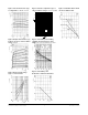
Figure 1. Current transfer ratio (typ.)
vs. temperature
I
F
=10 mA, V
CE
=5 V
Figure 2. Output characteristics (typ.)
Collector current vs. collector-emitter
voltage
T
A
=25°C
Figure 3. Diode forward voltage
(typ.) vs. forward current
Figure 7. Permissible diode forward
current vs. ambient temp.
Figure 4. Transistor capacitance (typ.) vs.
collector-emitter voltage
T
A
=25°C, f=1 MHz
Figure 5. Permissible pulse handling
capability. Forward current vs. pulse
width
Pulse cycle D=parameter, T
A
=25°C
Figure 6. Permissible power
dissipation vs. ambient temperature
20
15
10
0
5
pF
C
10
-2
10
-1
10
-0
10
1
10
2
V
V
e
C
CE