
Datasheet

SiHG22N60EF
www.vishay.com
Vishay Siliconix
S19-0120-Rev. A, 04-Feb-2019
2
Document Number: 92246
For technical questions, contact: hvm@vishay.com
THIS DOCUMENT IS SUBJECT TO CHANGE WITHOUT NOTICE. THE PRODUCTS DESCRIBED HEREIN AND THIS DOCUMENT
ARE SUBJECT TO SPECIFIC DISCLAIMERS, SET FORTH AT www.vishay.com/doc?91000
Notes
a. C
oss(er)
is a fixed capacitance that gives the same energy as C
oss
while V
DS
is rising from 0 % to 80 % V
DSS
b. C
oss(tr)
is a fixed capacitance that gives the same charging time as C
oss
while V
DS
is rising from 0 % to 80 % V
DSS
THERMAL RESISTANCE RATINGS
PARAMETER SYMBOL TYP. MAX. UNIT
Maximum junction-to-ambient R
thJA
-40
°C/W
Maximum junction-to-case (drain) R
thJC
-0.7
SPECIFICATIONS (T
J
= 25 °C, unless otherwise noted)
PARAMETER SYMBOL TEST CONDITIONS MIN. TYP. MAX. UNIT
Static
Drain-source breakdown voltage V
DS
V
GS
= 0 V, I
D
= 250 μA 600 - - V
V
DS
temperature coefficient V
DS
/T
J
Reference to 25 °C, I
D
= 1 mA - 0.68 - V/°C
Gate-source threshold voltage (N) V
GS(th)
V
DS
= V
GS
, I
D
= 250 μA 2.0 - 4.0 V
Gate-source leakage I
GSS
V
GS
= ± 20 V - - ± 100 nA
V
GS
= ± 30 V - - ± 1 μA
Zero gate voltage drain current I
DSS
V
DS
= 480 V, V
GS
= 0 V - - 1
μA
V
DS
= 480 V, V
GS
= 0 V, T
J
= 125 °C - - 500
Drain-source on-state resistance R
DS(on)
V
GS
= 10 V I
D
= 11 A - 0.158 0.182
Forward transconductance
a
g
fs
V
DS
= 30 V, I
D
= 11 A - 5.8 - S
Dynamic
Input capacitance C
iss
V
GS
= 0 V,
V
DS
= 100 V,
f = 1 MHz
- 1423 -
pF
Output capacitance C
oss
-73-
Reverse transfer capacitance C
rss
-5-
Effective output capacitance, energy
related
a
C
o(er)
V
DS
= 0 V to 480 V, V
GS
= 0 V
-48-
Effective output capacitance, time
related
b
C
o(tr)
- 240 -
Total gate charge Q
g
V
GS
= 10 V I
D
= 11 A, V
DS
= 480 V
-4896
nC Gate-source charge Q
gs
-9-
Gate-drain charge Q
gd
-21-
Turn-on delay time t
d(on)
V
DD
= 480 V, I
D
= 11 A,
V
GS
= 10 V, R
g
= 9.1
-1530
ns
Rise time t
r
-2142
Turn-off delay time t
d(off)
-5887
Fall time t
f
-2550
Gate input resistance R
g
f = 1 MHz, open drain 0.3 0.6 1.2
Drain-Source Body Diode Characteristics
Continuous source-drain diode current I
S
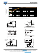
MOSFET symbol
showing the
integral reverse
p - n junction diode
--19
A
Pulsed diode forward current I
SM
--46
Diode forward voltage V
SD
T
J
= 25 °C, I
S
= 11 A, V
GS
= 0 V - - 1.2 V
Reverse recovery time t
rr
T
J
= 25 °C, I
F
= I
S
= 11 A,
di/dt = 100 A/μs, V
R
= 400 V
- 113 226 ns
Reverse recovery charge Q
rr
-0.71.4μC
Reverse recovery current I
RRM
-11-A
S
D
G