
Datasheet

SiHG22N60EF
www.vishay.com
Vishay Siliconix
S19-0120-Rev. A, 04-Feb-2019
5
Document Number: 92246
For technical questions, contact: hvm@vishay.com
THIS DOCUMENT IS SUBJECT TO CHANGE WITHOUT NOTICE. THE PRODUCTS DESCRIBED HEREIN AND THIS DOCUMENT
ARE SUBJECT TO SPECIFIC DISCLAIMERS, SET FORTH AT www.vishay.com/doc?91000
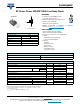
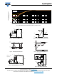
Fig. 12 - Normalized Transient Thermal Impedance, Junction-to-Case
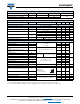
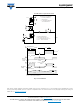
Fig. 13 - Switching Time Test Circuit
Fig. 14 - Switching Time Waveforms
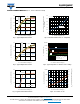
Fig. 15 - Unclamped Inductive Test Circuit
Fig. 16 - Unclamped Inductive Waveforms
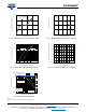
Fig. 17 - Basic Gate Charge Waveform
Fig. 18 - Gate Charge Test Circuit
10
10
10
10
0.01
0.1
1
0.0001 0.001 0.01 0.1 1
Axis Title
Normalized Effective Transient
Thermal Impedance
Pulse Time (s)
Duty cycle = 0.5
0.2
0.02
0.05
0.1
Single pulse
Pulse width ≤ 1 μs
Duty factor ≤ 0.1 %
R
D
V
GS
R
g
D.U.T.
10 V
+
-
V
DS
V
DD
V
DS
90 %
10 %
V
GS
t
d(on)
t
r
t
d(off)
t
f
R
g
I
AS
0.01 Ω
t
p
D.U.T.
L
V
DS
+
-
V
DD
10 V
Vary t
p
to obtain
required I
AS
I
AS
V
DS
V
DD
V
DS
t
p
Q
gs
Q
gd
Q
g
V
G
Charge
10 V
D.U.T.
3 mA
V
GS
V
DS
I
G
I
D
0.3 μF
0.2 μF
50 kΩ
12 V
Current regulator
Current sampling resistors
Same type as D.U.T.
+
-