
Datasheet

SMBJ5.0D thru SMBJ188D, SMBJ5.0CD thru SMBJ120CD
www.vishay.com
Vishay General Semiconductor
Revision: 16-Jan-18
3
Document Number: 87606
For technical questions within your region: DiodesAmericas@vishay.com
, DiodesAsia@vishay.com, DiodesEurope@vishay.com
THIS DOCUMENT IS SUBJECT TO CHANGE WITHOUT NOTICE. THE PRODUCTS DESCRIBED HEREIN AND THIS DOCUMENT
ARE SUBJECT TO SPECIFIC DISCLAIMERS, SET FORTH AT www.vishay.com/doc?91000
Notes
(1)
Mounted on minimum recommended pad layout
(2)
Mounted on 5.0 mm x 5.0 mm copper pad area
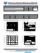
RATINGS AND CHARACTERISTICS CURVES (T
A
= 25 °C unless otherwise noted)
Fig. 1 - Peak Pulse Power Rating Curve
Fig. 2 - Pulse Power or Current vs. Initial Junction Temperature
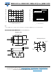
Fig. 3 - Pulse Waveform
Fig. 4 - Typical Junction Capacitance
THERMAL CHARACTERISTICS (T
A
= 25 °C unless otherwise noted)
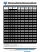
PARAMETER SYMBOL VALUE UNIT
Typical thermal resistance, junction to ambient
R
JA
(1)
125
°C/WR
JA
(2)
100
Typical thermal resistance, junction to mount R
JM
20
ORDERING INFORMATION (Example)
PREFERRED P/N UNIT WEIGHT (g) PREFERRED PACKAGE CODE BASE QUANTITY DELIVERY MODE
SMBJ5.0D-M3/H 0.096 H 750 7" diameter plastic tape and reel
SMBJ5.0D-M3/I 0.096 I 3200 13" diameter plastic tape and reel
0.1
1
10
10 100 1000 10 000
P
PPM
- Peak Pulse Power (kW)
t
d
-Pulse Width (μs)
0.2" x 0.2" (5.0 mm x 5.0 mm)
copper pad areas
0
25
50
75
100
0255075100125150
Peak Pulse Power (P
PP
) or Current (I
PP
)
Derating in Percentage, %
T
J
- Initial Temperature (°C)
0
50
100
150
0 0.5 1.0 1.5 2.0 2.5 3.0 3.5 4.0
I
PPM
- Peak Pulse Current, % I
RSM
t
p
-Time (ms)
T
J
= 25 °C
pulse width (t
d
) is de ned
as the point where the peak
current decays to 50 % of I
PPM
t
d
t
r
= 10 μs
Peak value I
PPM
Half value - I
PP
/2
10/1000 μs waveform
as de
ned by R.E.A.
1
10
100
1000
10000
110100
C
J
- Junction Capacitance (pF)
V
WM
- Reverse Stand-Off Voltage (V)
Measured at stand-off
voltage, V
WM
Measured at zero bias
T
J
= 25 °C
f = 1.0 MHz
Uni-Directional
Bi-Directional