
Datasheet

SMBJ5.0D thru SMBJ188D, SMBJ5.0CD thru SMBJ120CD
www.vishay.com
Vishay General Semiconductor
Revision: 16-Jan-18
4
Document Number: 87606
For technical questions within your region: DiodesAmericas@vishay.com
, DiodesAsia@vishay.com, DiodesEurope@vishay.com
THIS DOCUMENT IS SUBJECT TO CHANGE WITHOUT NOTICE. THE PRODUCTS DESCRIBED HEREIN AND THIS DOCUMENT
ARE SUBJECT TO SPECIFIC DISCLAIMERS, SET FORTH AT www.vishay.com/doc?91000
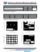
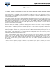
Fig. 5 - Power Dissipation Derating Curve Fig. 6 - Typical Transient Thermal Impedance
Note
• Fig.1, 10 000 μs P
ppm
is actual test for V
WM
60 V types, over 60 V types 10 000 μs P
ppm
is curve extensional value
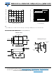
PACKAGE OUTLINE DIMENSIONS in inches (millimeters)
0
1
2
3
4
5
6
0 255075100125150
P
M(av)
- Steady State Power Dissipation (W)
T
A
- Ambient Temperature (°C)
T
A
=T
M
mounted on ininite heatsink
Mounted on minimum
recommend pad layout
0.1
1
10
100
1000
0.001 0.1 10 1000
Transient Thermal Impedance (°C/W)
t
p
-Pulse Duration (s)
Junction to Ambient
Mounted on minimum
recommend pad area
Mounted on 5.0 x 5.0 mm
copper pad area
SMB (DO-214AA)
0.160 (4.06)
0.180 (4.57)
0.006 (0.152)
0.012 (0.305)
0.030 (0.76)
0.060 (1.52)
0.205 (5.21)
0.220 (5.59)
0 (0)
0.008 (0.2)
0.130 (3.30)
0.155 (3.94)
0.084 (2.13)
0.096 (2.44)
0.077 (1.95)
0.086 (2.20)
Cathode Band
Mounting Pad Layout
0.085 (2.159)
MAX.
0.220 REF.
0.086 (2.18)
MIN.
0.060 (1.52)
MIN.