
Datasheet

TCLD1000
www.vishay.com
Vishay Semiconductors
Rev. 2.0, 21-Mar-14
2
Document Number: 83516
For technical questions, contact: optocoupleranswers@vishay.com
THIS DOCUMENT IS SUBJECT TO CHANGE WITHOUT NOTICE. THE PRODUCTS DESCRIBED HEREIN AND THIS DOCUMENT
ARE SUBJECT TO SPECIFIC DISCLAIMERS, SET FORTH AT www.vishay.com/doc?91000
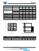
Notes
• Stresses in excess of the absolute maximum ratings can cause permanent damage to the device. Functional operation of the device is not
implied at these or any other conditions in excess of those given in the operational sections of this document. Exposure to absolute
maximum ratings for extended periods of the time can adversely affect reliability.
(1)
Wave soldering three cycles are allowed. Also refer to “Assembly Instructions” (www.vishay.com/doc?80054).
Note
• Minimum and maximum values are tested requierements. Typical values are characteristics of the device and are the result of engineering
evaluations. Typical values are for information only and are not part of the testing requirements.
OUTPUT
Collector emitter voltage V
CEO
35 V
Emitter collector voltage V
ECO
7V
Collector current I
C
80 mA
Collector peak current t
p
/T = 0.5, t
p
≤ 10 ms I
CM
100 mA
Power dissipation P
diss
150 mW
Junction temperature T
j
125 °C
COUPLER
Isolation test voltage (RMS) V
ISO
5000 V
RMS
Total power dissipation P
tot
250 mW
Operating ambient temperature range T
amb
-55 to +100 °C
Storage temperature range T
stg
-55 to +150 °C
Soldering temperature
(1)
T
sld
260 °C
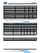
ELECTRICAL CHARACTERISTICS (T
amb
= 25 °C, unless otherwise specified)
PARAMETER TEST CONDITION SYMBOL MIN. TYP. MAX. UNIT
INPUT
Forward voltage I
F
= 20 mA V
F
1.1 1.4 V
Junction capacitance V
R
= 0 V, f = 1 MHz C
j
50 pF
OUTPUT
Collector emitter voltage I
C
= 1 mA V
CEO
32 V
Emitter collector voltage I
E
= 100 μA V
ECO
7V
Collector ermitter leakage current V
CE
= 10 V, IF = 0 A I
CEO
15 100 nA
COUPLER
Collector emitter saturation voltage I
F
= 20 mA, I
C
= 5 mA V
CEsat
1V
Cut-off frequency
V
CE
= 5 V, I
F
= 10 mA,
R
L
= 100 Ω
f
c
10 kHz
Coupling capacitance f = 1 MHz C
k
0.3 pF
CURRENT TRANSFER RATIO (T
amb
= 25 °C, unless otherwise specified)
PARAMETER TEST CONDITION SYMBOL MIN. TYP. MAX. UNIT
I
C
/I
F
V
CE
= 2 V, I
F
= 1 mA CTR 600 800 %
ABSOLUTE MAXIMUM RATINGS (T
amb
= 25 °C, unless otherwise specified)
PARAMETER TEST CONDITION SYMBOL VALUE UNIT