
Datasheet

TCLD1000
www.vishay.com
Vishay Semiconductors
Rev. 2.0, 21-Mar-14
3
Document Number: 83516
For technical questions, contact: optocoupleranswers@vishay.com
THIS DOCUMENT IS SUBJECT TO CHANGE WITHOUT NOTICE. THE PRODUCTS DESCRIBED HEREIN AND THIS DOCUMENT
ARE SUBJECT TO SPECIFIC DISCLAIMERS, SET FORTH AT www.vishay.com/doc?91000
Note
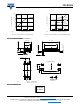
• According to DIN EN 60747-5-2 (VDE 0884) (see figure 2). This optocoupler is suitable for safe electrical isolation only within the safety
ratings. Compliance with the safety ratings shall be ensured by means of suitable protective circuits.
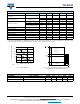
Fig. 1 - Derating Diagram Fig. 2 - Test Pulse Diagram for Sample Test According to
DIN EN 60747-5-2 (VDE 0884); IEC 60747-5-5
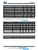
SAFETY AND INSULATION RATED PARAMETERS
PARAMETER TEST CONDITION SYMBOL MIN. TYP. MAX. UNIT
Partial discharge test voltage -
routine test
100 %, t
test
= 1 s V
pd
2kV
Partial discharge test voltage -
lot test (sample test)
t
Tr
= 60 s, t
test
= 10 s,
(see figure 2)
V
IOTM
8kV
V
pd
1.68 kV
Insulation resistance
V
IO
= 500 V R
IO
10
12
Ω
V
IO
= 500 V, T
amb
= 100 °C R
IO
10
11
Ω
V
IO
= 500 V, T
amb
= 150 °C
(construction test only)
R
IO
10
9
Ω
Forward current I
si
130 mA
Power dissipation P
so
265 mW
Rated impulse voltage V
IOTM
8kV
Safety temperature T
si
150 °C
Clearance distance 8.0 mm
Creepage distance 8.0 mm
Insulation distance (internal) 0.40 mm
0
50
100
150
200
250
300
0 40 80 120
P
tot
- Total Power Dissipation (mW)
T
amb
- Ambient Temperature (°C)
96 11700
Coupled device
Phototransistor
IR-diode
t
13930
t
1
, t
2
= 1 s to 10 s
t
3
, t
4
= 1 s
t
test
= 10 s
t
stres
= 12 s
V
IOTM
V
pd
V
IOWM
V
IORM
0
t
1
t
test
t
Tr
= 60 s
t
stres
t
3
t
4
t
2
SWITCHING CHARACTERISTICS (T
amb
= 25 °C, unless otherwise specified)
PARAMETER TEST CONDITION SYMBOL MIN. TYP. MAX. UNIT
Rise time V
CE
= 2 V, I
C
= 10 mA, R
L
= 100 Ω, (see figure 3) t
r
300 μs
Turn-off time V
CE
= 2 V, I
C
= 10 mA, R
L
= 100 Ω, (see figure 3) t
off
250 μs